Thin Semiconductor Device And Operation Method Of Thin Semiconductor Device

a thin semiconductor and operation method technology, applied in the field of thin semiconductor devices, can solve problems such as inability to prevent information leakage, and achieve the effects of enhancing preventing falsification, and improving the security of a thin semiconductor devi

Inactive Publication Date: 2007-11-29
SEMICON ENERGY LAB CO LTD
View PDF13 Cites 36 Cited by
  • Summary
  • Abstract
  • Description
  • Claims
  • Application Information

AI Technical Summary

Benefits of technology

[0015] According to the present invention, the security of a thin semiconductor device can be improved. According to the present invention, a new operation method of a thin semiconductor device can be provided. In the operation method of the present invention, the memory can be a nonvolatile memory. Using the nonvolatile memory that can write to only once can prevent falsification. The nonvolatile memory can further enhance the security of a thin semiconductor device.
[0016] In the operation method of the present invention, the memory can be a rewritable memory. Thus, the thin film integrated circuit can be reused to contrib

Problems solved by technology

No measures for preventing info

Method used


Image

  • Thin Semiconductor Device And Operation Method Of Thin Semiconductor Device
  • Thin Semiconductor Device And Operation Method Of Thin Semiconductor Device
  • Thin Semiconductor Device And Operation Method Of Thin Semiconductor Device

Examples


embodiment mode 1

[0039] Embodiment Mode 1 describes an operation method of a thin semiconductor device in which a plurality of thin film integrated circuits are mounted.

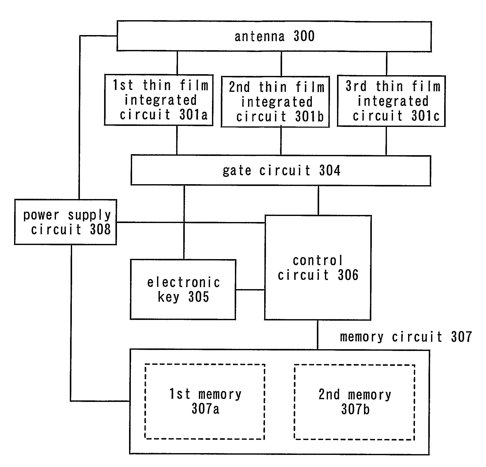
[0040] As shown in FIG. 1, in a thin semiconductor device of this embodiment mode, a first thin film integrated circuit 301a, a second thin film integrated circuit 301b and a third thin film integrated circuit 301c that share an antenna 300, are connected to an electronic key 305 and a control circuit 306 through a gate circuit 304. The electronic key 305 may be formed by using a nonvolatile memory. This is because falsification of the electronic key itself and abuse accompanied with it can be prevented. A memory circuit 307 includes a first memory 307a and a second memory 307b, and is connected to the control circuit 306. Note that the first memory 307a and the second memory 307b are shown for convenience; however, a region for forming the memories is not necessarily divided in the actual memory circuit 307. The antenna 300, the co...

embodiment mode 2

[0060] In Embodiment Mode 2, an operation method of a thin semiconductor device is described. The operation method is different from that of Embodiment Mode 1 in an update method of key information. As shown in FIG. 4, in the thin semiconductor device of this embodiment mode, a first thin film integrated circuit 301a and a second thin film integrated circuit 301b that share an antenna 300, are connected to an electronic key 305 and a control circuit 306 through a gate circuit 304. The electronic key 305 may be formed from a nonvolatile memory. This is because falsification of the electronic key itself and abuse accompanied with it can be prevented. A memory circuit 307 is connected to the control circuit 306. Note that the memory circuit 307 may include a first memory 307a and a second memory 307b. In addition, the antenna 300, the control circuit 306 and the memory circuit 307 are each connected to a power supply circuit 308.

[0061] An operation method of the above described thin s...

embodiment mode 3

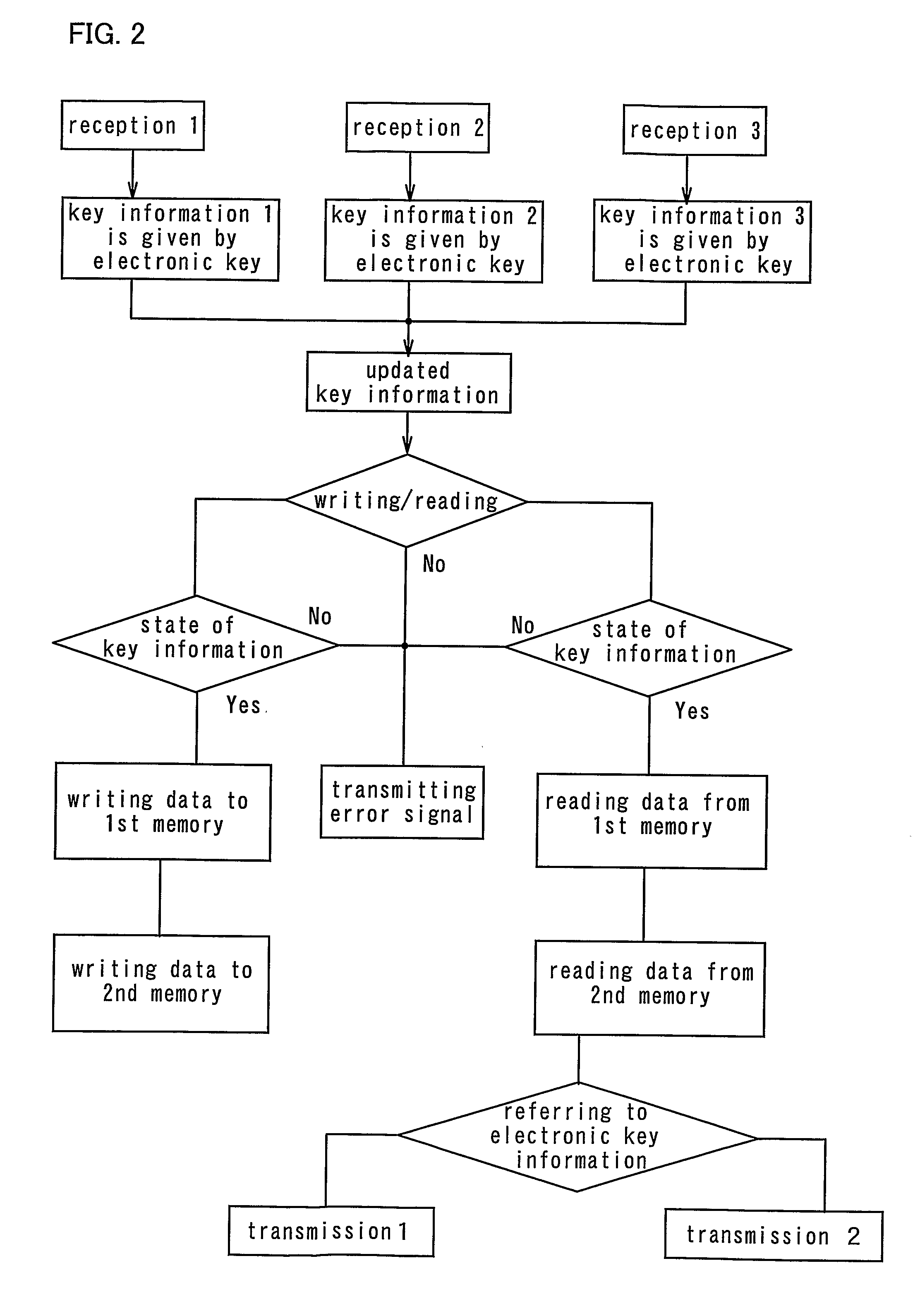
[0069] Embodiment Mode 3 describes a communication system (communication mode) between a thin film integrated circuit and a reader / writer by using a flow chart shown in FIG. 7.

[0070] A thin semiconductor device is brought close to a reader / writer. At this time, a thin film integrated circuit C1 of the thin semiconductor device receives a signal. Thus, writing or the like to a memory circuit in the thin semiconductor device is conducted. Thereafter, information is sent from the thin film integrated circuit C1 to the reader / writer. Then, the reader / writer determines whether to communicate with another thin film integrated circuit Cn.

[0071] After that, communication with another thin film integrated circuit Cn is conducted, information is sent to the reader / writer from the thin film integrated circuit Cn. Thereafter, the reader / writer determines whether to communicate with another thin film integrated circuit.

[0072] Whether communication with another thin film integrated circuit is ...


PUM


Abstract

The present invention provides a thin semiconductor device in which its security such as prevention of counterfeit or information leakage is to be enhanced. One feature of the present invention is a thin semiconductor device in which a plurality of thin film integrated circuits are mounted and in which at least one integrated circuit is different from the other integrated circuits in any one of a specification, layout, frequency for transmission or reception, a memory, a communication means, a communication rule and the like. According to the present invention, a thin semiconductor device tag having the plurality of thin film integrated circuits communicates with a reader/writer and at least one of the thin film integrated circuits receives a signal to write information in a memory, and the information written in the memory determines which of the thin film integrated circuits communicates.

Description

TECHNICAL FIELD [0001] The present invention relates to a thin semiconductor device in which a thin film integrated circuit is mounted and an operation method of the thin semiconductor device. BACKGROUND ART [0002] As for a conventional non-contact IC card, there is proposed a structure in which capacity adjustment of a capacitor for setting the resonance frequency of a resonant circuit in an antenna mechanism is not required, mechanical damages to elements constituting a card are minimalized, and mass-productivity is increased. The structure has a plane coil which is connected to a non-contact IC chip and plural other plane coils which are arranged in the periphery thereof (References 1: Japanese Patent Laid-Open No. 2001-109861 and Reference 2: Japanese Patent Laid-Open No. 2001-109862). According to References 1 and 2, each of resonance frequencies is a frequency of high frequency electromagnetic field from a reader / writer device, a frequency shifted up / down to some extent, or th...

Claims


Application Information

Patent Timeline
IPC IPC(8): G06K19/077H01L29/94B42D15/10G06K7/00G06K17/00G06K19/07
CPCG06K19/07718G06K7/0008G06K19/072G06K19/0723G06K19/07749
Inventor YAMAZAKI, SHUNPEIOSADA, TAKESHIARAI, YASUYUKITACHIMURA, YUKO
Owner SEMICON ENERGY LAB CO LTD
Why Eureka
Try Eureka