RF and/or RF identification tag/device having an integrated interposer, and methods for making and using the same

a technology of integrated interposer and identification tag, which is applied in the field of sensors, electronic article surveillance (eas), radio frequency (rf) and/or rf identification (rfid) tags and devices, can solve the problems of relatively slow and expensive process of physical and electrical interconnection, and achieve low capital expenditure and operating costs of equipment, increase material utilization, and achieve cost advantages

Inactive Publication Date: 2007-11-29
ENSURGE MICROPOWER ASA
View PDF77 Cites 70 Cited by
  • Summary
  • Abstract
  • Description
  • Claims
  • Application Information

AI Technical Summary

Benefits of technology

[0021] One potential approach to producing very low-cost RFID tags may use printing techniques in a web- or sheet-fed process. Printing has potential cost advantages, since it can increase materials utilization (e.g., additive or semi-additive processing), combine deposition and patterning steps, and leverage low capital expenditures and operating costs for equipment. Furthermore, high throughput conventional printing processes can be adapted to flexible substrates (e.g., a plastic sheet or a metal foil), improving tag uses in a number of applications. The materials efficiency and additive processing approaches enables a lower cost per unit area of processed interposers (or die, when used), which enables low cost attach processing and/or integration of passive devices with the active circuitry. Also, mask-less processes such as printing enable facile customization of RF devices, for example where each individual RF device is provided with a unique identification code and/or a unique response time delay with respect to a reader inquiry.
[0022] Furthermore, if circuitry can be directly printed on the antenna or inductor structure itself, the attach steps and related costs can be eliminated. This approach diverges from the conventional semiconductor wafer cost reduction approach of reducing die cost by decreasing die size (although this approach may become self-limiting for direct-attached Si RFID tags, as the attach costs increase for smaller die). However, a fully-printed, non-area constrained RFID tag may further benefit from development of certain processes, tools, and/or materials that may not be widely or commercially available. The “integrated interposer” approach outlined herein allows for the combination of printing and low cost per unit area display processing (e.g., 0.35 micron Si die processing costs are presently about $25/in2; conventional display polysilicon processing costs are about $0.50-$0.90/in2; and printing-based processing is expected to cost<<$0.50/in2).
[0023] By using an interposer-based process, some or al...

Problems solved by technology

As a whole, the process of picking out a separated (sawn) die, moving it to the right place on the antenna(e), inductor, carrier, or interposer to which it is t...

Method used


Image

  • RF and/or RF identification tag/device having an integrated interposer, and methods for making and using the same
  • RF and/or RF identification tag/device having an integrated interposer, and methods for making and using the same
  • RF and/or RF identification tag/device having an integrated interposer, and methods for making and using the same

Examples


Embodiment Construction

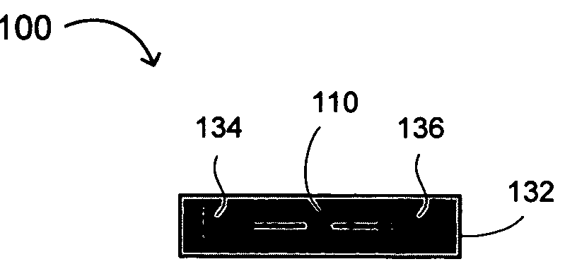
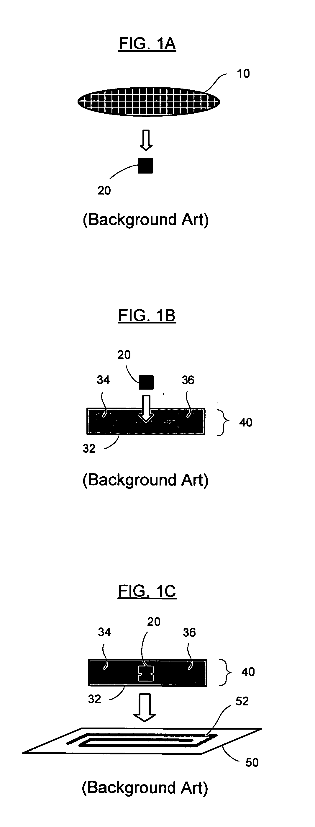
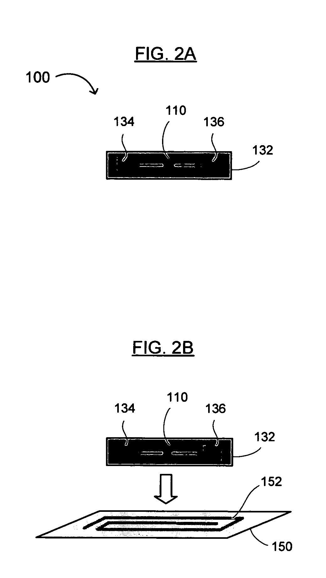
[0028] Reference will now be made in detail to the preferred embodiments of the invention, examples of which are illustrated in the accompanying drawings. While the invention will be described in conjunction with the preferred embodiments, it will be understood that they are not intended to limit the invention to these embodiments. On the contrary, the invention is intended to cover alternatives, modifications and equivalents, which may be included within the spirit and scope of the invention as defined by the appended claims. Furthermore, in the following detailed description of the present invention, numerous specific details are set forth in order to provide a thorough understanding of the present invention. However, it will be readily apparent to one skilled in the art that the present invention may be practiced without these specific details. In other instances, well-known methods, procedures, components, and circuits have not been described in detail so as not to unnecessarily...


PUM

PropertyMeasurementUnit
Lengthaaaaaaaaaa
Lengthaaaaaaaaaa
Lengthaaaaaaaaaa

Abstract

A MOS RF surveillance and/or identification tag, and methods for its manufacture and use. The tag generally includes an interposer, an antenna and/or inductor on the interposer, and integrated circuitry on the interposer in a location other than the antenna and/or inductor. The integrated circuitry generally has a lowest layer in physical contact with the interposer surface. The method of manufacture generally includes forming a lowest layer of integrated circuitry on an interposer, forming successive layers of the integrated circuitry on the lowest layer of integrated circuitry, and attaching an electrically conductive functional layer to the interposer. Alternatively, an electrically conductive structure may be formed from a functional layer attached to the interposer. The method of use generally includes causing and/or inducing a current in the present tag sufficient for it to generate, reflect or modulate a detectable electromagnetic signal, detecting the signal, and optionally, processing information conveyed by the detectable electromagnetic signal. The present invention advantageously provides a low cost RFID tag capable of operating at MHz frequencies that can be manufactured in a shorter time period than conventional RFID tags that manufacture all active electrical devices on a conventional wafer.

Description

RELATED APPLICATIONS [0001] This application claims the benefit of U.S. Provisional Application No. 60 / 617,617, filed Oct. 8, 2004 (Attorney Docket No. IDR0271), which is incorporated herein by reference in its entirety.FIELD OF THE INVENTION [0002] The present invention generally relates to the field of sensors, electronic article surveillance (EAS), radio frequency (RF) and / or RF identification (RFID) tags and devices. More specifically, embodiments of the present invention pertain to EAS, RF and / or RFID structures and methods for their manufacturing and / or production. As a result, the present invention may provide a low-cost process for producing an RFID (or EAS) tag comprising a substrate, an RF front end or subset of an RF front end, memory and logic circuit. DISCUSSION OF THE BACKGROUND [0003] Remotely powered electronic devices and related systems are known. For example, U.S. Pat. No. 5,099,227, issued to Geiszler et al. and entitled “Proximity Detecting Apparatus,” discloses...

Claims


Application Information

Patent Timeline
IPC IPC(8): G08B13/14
CPCG06K19/07749G06K19/0775Y10T29/43G08B13/2437Y10T29/435G08B13/2417G06K19/07752
Inventor MACKENZIE, J. DEVINPAVATE, VIKRAM
Owner ENSURGE MICROPOWER ASA
Why Eureka
Try Eureka