Back side wafer dicing

a wafer and back side technology, applied in the field of dicing a wafer, can solve the problems of laser dicing damage to the ics b>110/b>, more edge chipping, and unprotected top surface of the ics b>110/b>, and achieve the effect of reducing or no damage or debris

Inactive Publication Date: 2007-11-29
ELECTRO SCI IND INC
View PDF11 Cites 42 Cited by
  • Summary
  • Abstract
  • Description
  • Claims
  • Application Information

AI Technical Summary

Benefits of technology

[0008]The embodiments disclosed herein provide systems and methods for scribing a semiconductor wafer with reduced or no damage or debris to a top surface of the semiconductor wafer caused by the scribing process. The semiconductor wafer is scribed from a back side

Problems solved by technology

However, the top surface of the ICs 110 are left unprotected during the dicing process and may be damaged by the mechanical saw or laser.
In addition, as thinner wafers are produced, mechanical saws cause more edge chipping.
Laser dicing can also damage the ICs 110 and reduce yield.
The process of laser dicing generates excessive heat and debris.
The heat

Method used


Image

  • Back side wafer dicing
  • Back side wafer dicing
  • Back side wafer dicing

Examples


Embodiment Construction

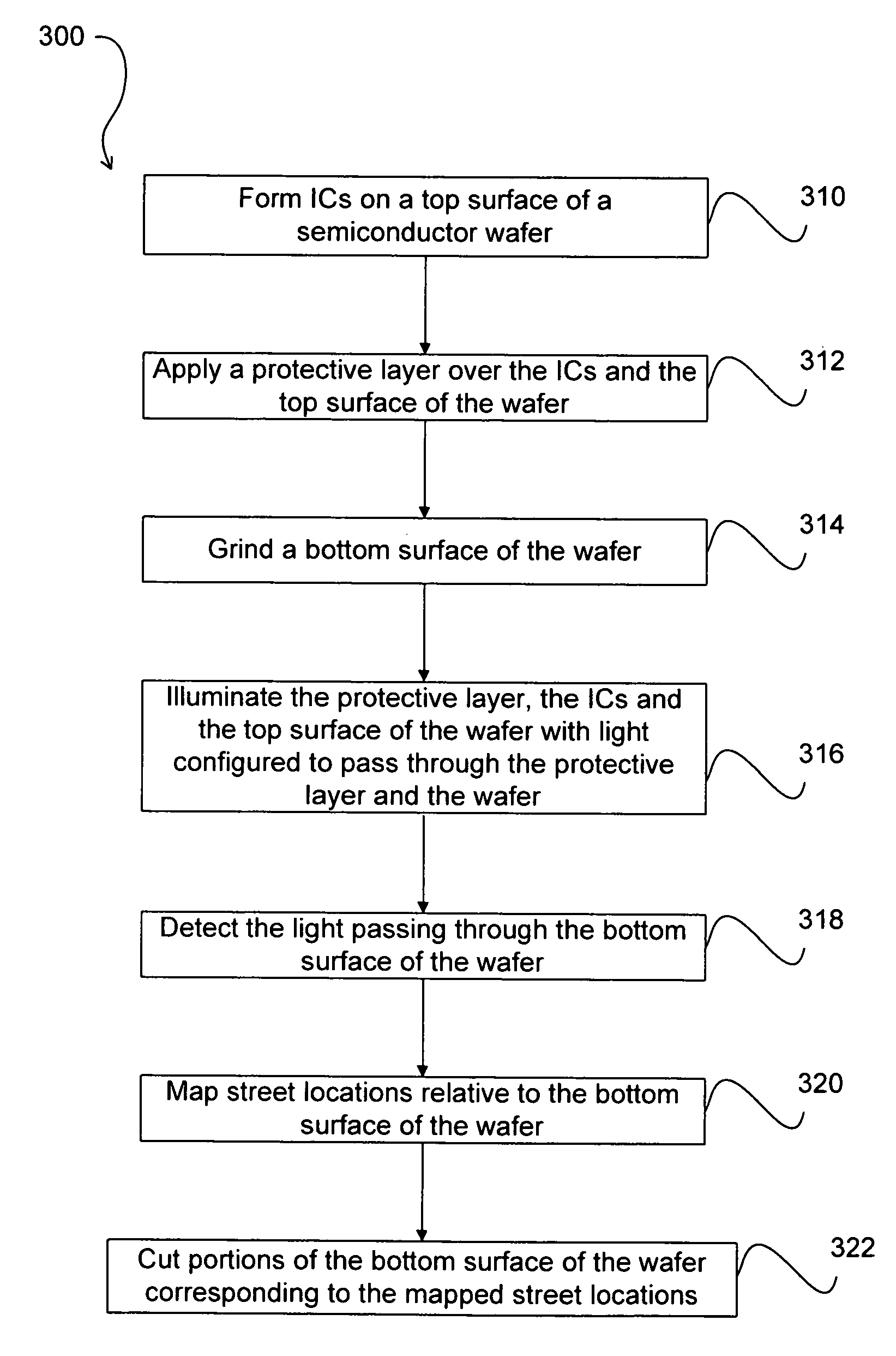
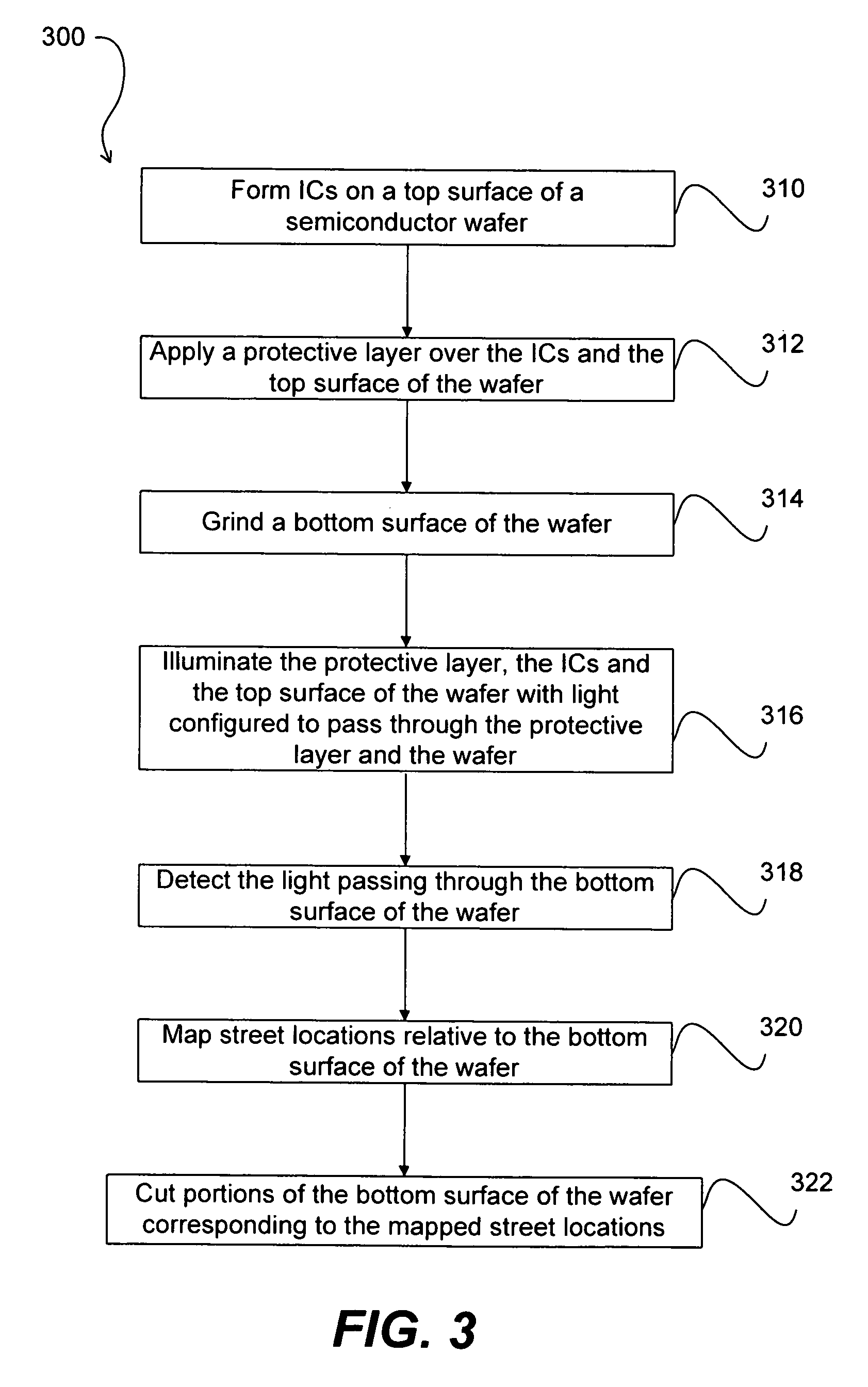
[0019]To avoid cutting metal features (e.g., test circuits) or other materials such as low-k dielectrics formed on a top surface of a semiconductor wafer, certain embodiments disclosed herein provide systems and methods for cutting the back side of the semiconductor wafer. The back side of the semiconductor surface is also referred to herein as the “bottom” or “bottom surface” and is generally on an opposite surface from the front or top surface where ICs and dicing lines or streets are formed.

[0020]For convenience, the term cutting may be used generically to include trenching (cutting that does not penetrate the full depth of a target work piece) and throughcutting, which includes slicing (often associated with wafer row separation) or dicing (often associated with part singulation from wafer rows). Slicing and dicing may be used interchangeably in the context of this disclosure.

[0021]As discussed above, the streets are generally visible from the top surface of the semiconductor wa...


PUM

PropertyMeasurementUnit
Wavelengthaaaaaaaaaa

Abstract

Systems and methods for scribing a semiconductor wafer with reduced or no damage or debris to or on individual integrated circuits caused by the scribing process. The semiconductor wafer is scribed from a back side thereof. In one embodiment, the back side of the wafer is scribed following a back side grinding process but prior to removal of back side grinding tape. Thus, debris generated from the scribing process is prevented from being deposited on a top surface of the wafer. To determine the location of dicing lanes or streets relative to the back side of the wafer, the top side of the wafer is illuminated with a light configured to pass through the grinding tape and the wafer. The light is detected from the back side of the wafer, and the streets are mapped relative to the back side. The back side of the wafer is then cut with a saw or laser.

Description

TECHNICAL FIELD [0001]This application relates to processing a wafer and, in particular, to a method and / or system for dicing a wafer from the back side thereof.BACKGROUND INFORMATION [0002]Integrated circuits (ICs) are generally fabricated in an array on or in a semiconductor substrate. For example, FIG. 1 is a perspective view of a typical semiconductor wafer 100 having a plurality of ICs 110 formed thereon. The ICs 110 are separated by dicing lines or streets 112 that form a lattice pattern on a top surface of the semiconductor wafer 100.[0003]The ICs 110 are singulated by mounting the back side of the semiconductor wafer 100 on a tape frame (not shown) and cutting along the streets 112 formed on the top surface of the semiconductor wafer 100. Cutting is generally carried out by a cutting machine called a dicer that includes a chuck table for holding the semiconductor wafer 100 and a mechanical saw or laser for cutting the semiconductor wafer 100. Mechanical saws generally includ...

Claims


Application Information

Patent Timeline
IPC IPC(8): H01L21/00
CPCB23K26/04B23K26/4075H01L21/78H01L21/67092B28D5/0011B23K26/40B23K2103/50H01L21/00
Inventor HARRIS, RICHARD S.LO, HO W.
Owner ELECTRO SCI IND INC
Why Eureka
Try Eureka