Optical waveguide with single sided coplanar contact optical phase modulator

a phase modulator and optical waveguide technology, applied in the field of optical modulation, can solve the problems of devices generally requiring relatively high voltages in order to switch optical beams, limiting the application of slower speed optical devices,

Inactive Publication Date: 2007-12-06
INTEL CORP
View PDF74 Cites 35 Cited by
  • Summary
  • Abstract
  • Description
  • Claims
  • Application Information

AI Technical Summary

Problems solved by technology

However, since MEMS technology generally relies upon the actual mechanical movement of physical parts or components, MEMS are generally limited to slower speed optical applications, such as for example applications having response times on the order of milliseconds.
Although the switching speeds of these types of devices are very fast, for example on the order of nanoseconds, one disadvantage with present day electro-optic switching devices is that these devices generally require relatively high voltages in order to switch optical beams.
Consequently, the external circuits utilized to control present day electro-optical switches are usually specially fabricated to generate the high voltages and suffer from large amounts of power consumption.
In addition, integration of these external high voltage control circuits with present day electro-optical switches is becoming an increasingly challenging task as device dimensions continue to scale down and circuit densities continue to increase.

Method used


Image

  • Optical waveguide with single sided coplanar contact optical phase modulator
  • Optical waveguide with single sided coplanar contact optical phase modulator
  • Optical waveguide with single sided coplanar contact optical phase modulator

Examples


Embodiment Construction

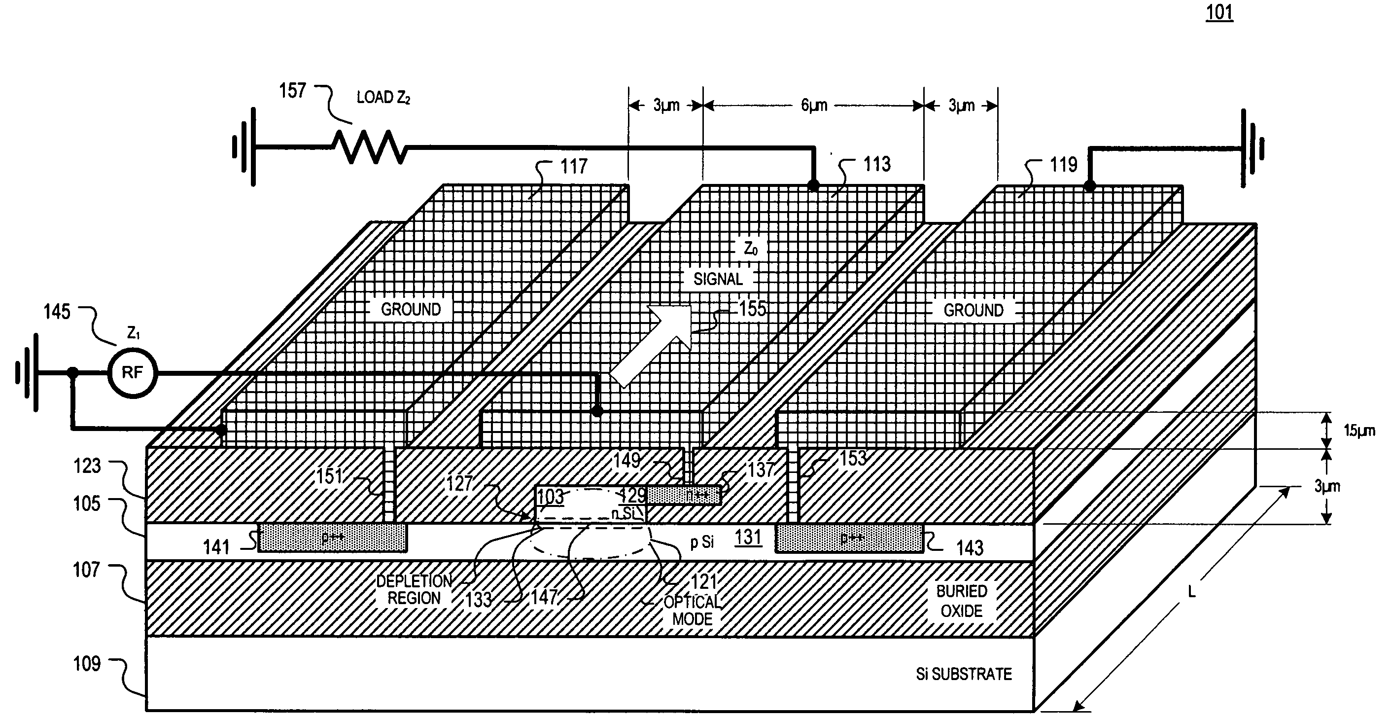
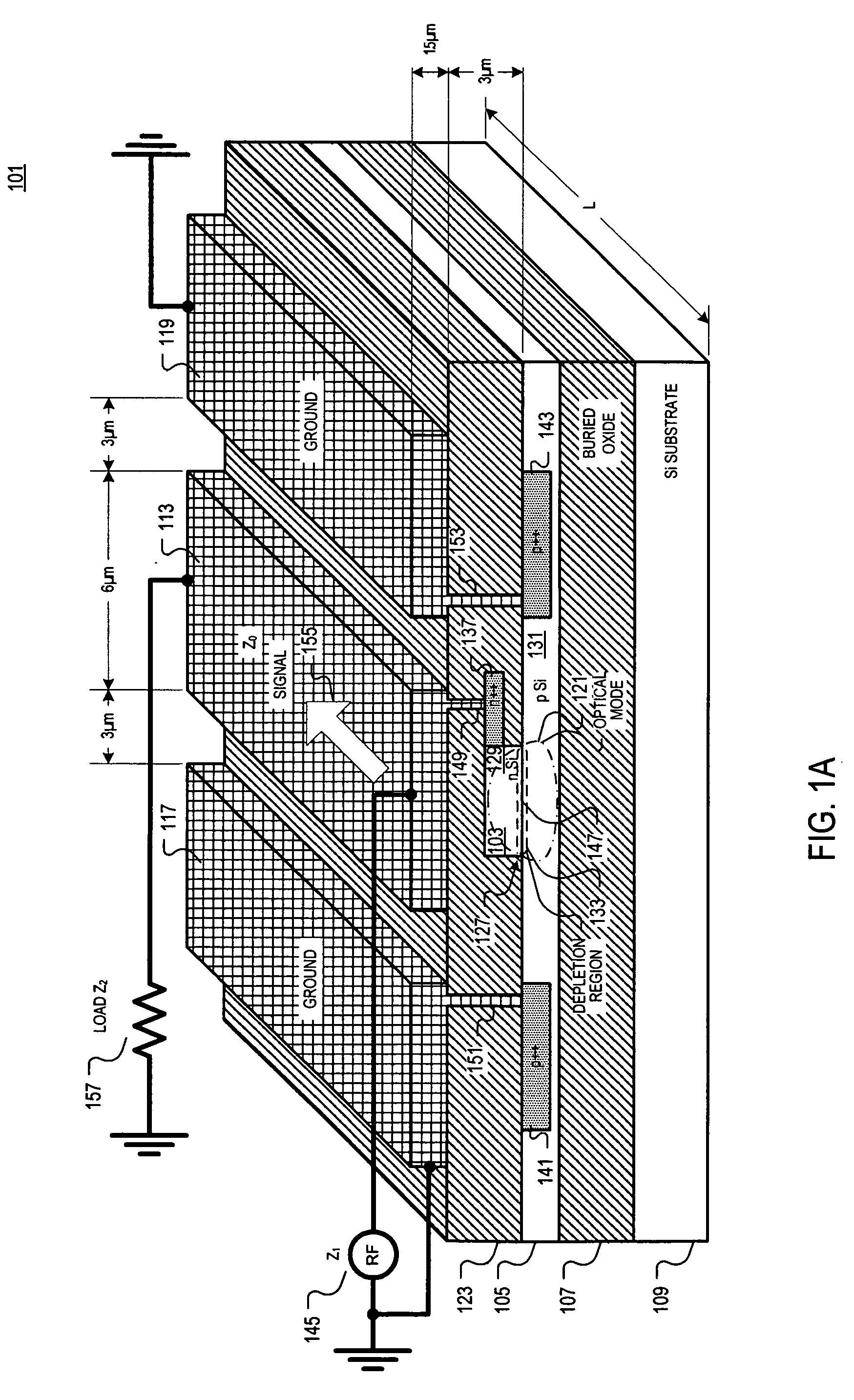
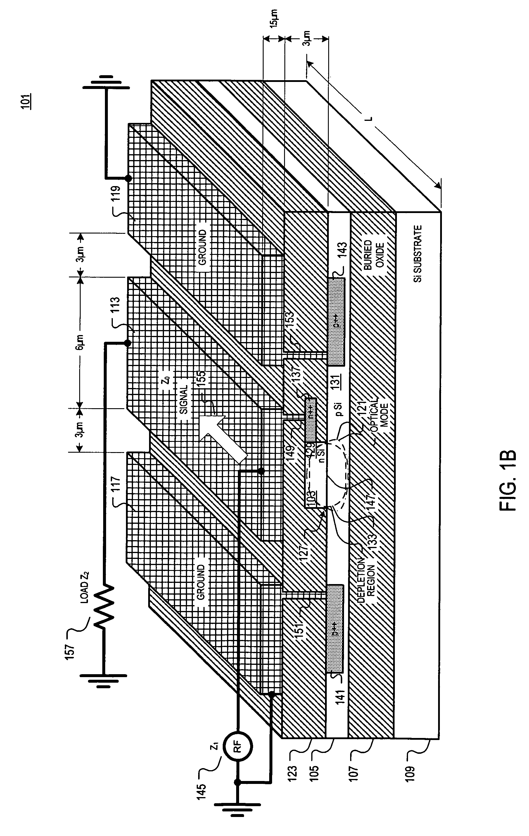
[0017]Methods and apparatuses for high speed phase shifting an optical beam with an optical device are disclosed. In the following description numerous specific details are set forth in order to provide a thorough understanding of the present invention. It will be apparent, however, to one having ordinary skill in the art that the specific detail need not be employed to practice the present invention. In other instances, well-known materials or methods have not been described in detail in order to avoid obscuring the present invention.

[0018]Reference throughout this specification to “one embodiment” or “an embodiment” means that a particular feature, structure or characteristic described in connection with the embodiment is included in at least one embodiment of the present invention. Thus, appearances of the phrases “in one embodiment” or “in an embodiment” in various places throughout this specification are not necessarily all referring to the same embodiment. Furthermore, the par...


PUM


Abstract

An apparatus and method for high speed phase modulation of optical beam. For one embodiment, an apparatus includes an optical waveguide having adjoining first and second regions disposed in semiconductor material. The first and second regions have opposite first and second doping types, respectively. First, second and third higher doped regions of semiconductor material outside an optical path of the optical waveguide are also included. The first higher doped region has the first doping type and the second and third higher doped regions have the second doping type. The first, second and third higher doped regions have higher doping concentrations than doping concentrations within the optical path of the optical waveguide. The second and third higher doped regions are symmetrically adjoining and coupled to respective opposite lateral sides of the second region. The first higher doped region is asymmetrically adjoining and coupled to only one of two opposite lateral sides of the first region. First, second and third coplanar contacts are also included and are coupled to the first, second and third higher doped regions, respectively.

Description

BACKGROUND OF THE INVENTION[0001]1. Field of the Invention[0002]The present invention relates generally to optics and, more specifically, the present invention relates to modulating optical beams.[0003]2. Background Information[0004]The need for fast and efficient optical-based technologies is increasing as Internet data traffic growth rate is overtaking voice traffic pushing the need for optical communications. Transmission of multiple optical channels over the same fiber in the dense wavelength-division multiplexing (DWDM) systems and Gigabit (GB) Ethernet systems provide a simple way to use the unprecedented capacity (signal bandwidth) offered by fiber optics. Commonly used optical components in the system include wavelength division multiplexed (WDM) transmitters and receivers, optical filter such as diffraction gratings, thin-film filters, fiber Bragg gratings, arrayed-waveguide gratings, optical add / drop multiplexers, lasers and optical switches. Optical switches may be used t...

Claims


Application Information

Patent Timeline
Patent Type & Authority Applications(United States)
IPC IPC(8): H01S3/10
CPCG02F1/025
Inventor LIU, ANSHENG
Owner INTEL CORP
Why Eureka
Try Eureka