Method and System for Detecting Analytes

a technology of analytes and detection methods, applied in the field of methods and systems for detecting and/or identifying analytes, can solve the problems of unable to achieve partial success, inability to develop microfluidic devices, and inability to conveniently and safely detect and measure low levels of compounds

Inactive Publication Date: 2007-12-06
YISSUM RES DEV CO OF THE HEBREWUNIVERSITY OF JERUSALEM LTD +1
View PDF0 Cites 133 Cited by
  • Summary
  • Abstract
  • Description
  • Claims
  • Application Information

AI Technical Summary

Benefits of technology

[0130] According to still further features in the described preferred embodiments the apparatus further comprises an additional optical element positioned betwe...

Problems solved by technology

Yet, there remain problems in detecting and measuring low levels of compounds conveniently, safely and quickly.
Heretofore, attempt to developed microfluidic devices for the purpose of detecting analysts, resulted in only partial success.
Purified enzymes are, however, expensive and unstable, thus limiting their applications in the field of biosensors.
Note, the major drawback of such an approach is the need to maintain at least two cultures of microorganisms on a single sensor which may prove problematic such as due to different nutritional needs.
The above technologies suffer from many limitations.
For example, in most prior art systems...

Method used


Image

  • Method and System for Detecting Analytes
  • Method and System for Detecting Analytes
  • Method and System for Detecting Analytes

Examples


example 1

CMOS Detector

[0382] Reference is now made to FIG. 22a-b exemplifying an electronic diagram of a CMOS detector 200, which can be used as detector 108, according to a preferred embodiment of the present invention. CMOS detector 200 is known in the art and can be purchased, for example, from Fill Factory, Mechelen Belgium.

[0383] CMOS detector 200 comprises a matrix 201 of elementary units 202 referred to herein as pixels 202. FIG. 22b shows one pixel 202, which comprises a capacitor 204 which is pre-charged to a reset bias voltage, a photodiode 206, for discharging capacitor 204 in response to photons absorption and 3 MOS transistors, designated 208a, 208b and 208c, for resetting (transistor 208a), sensing (transistor 208b) and leading (transistor 208c) the signal to column amplifier 210.

[0384] CMOS detector 200 further comprising a left vertical shift register 212 and a right vertical shift register 214. Left register 212 serves a pointer to a row that is pre-charged to reset bias ...

example 2

Determination of Analyte Concentration Using the Detected Signals

[0392] Reference is now made to FIGS. 23a-c, which illustrate the radiation emitted by one reaction chamber of device 10.

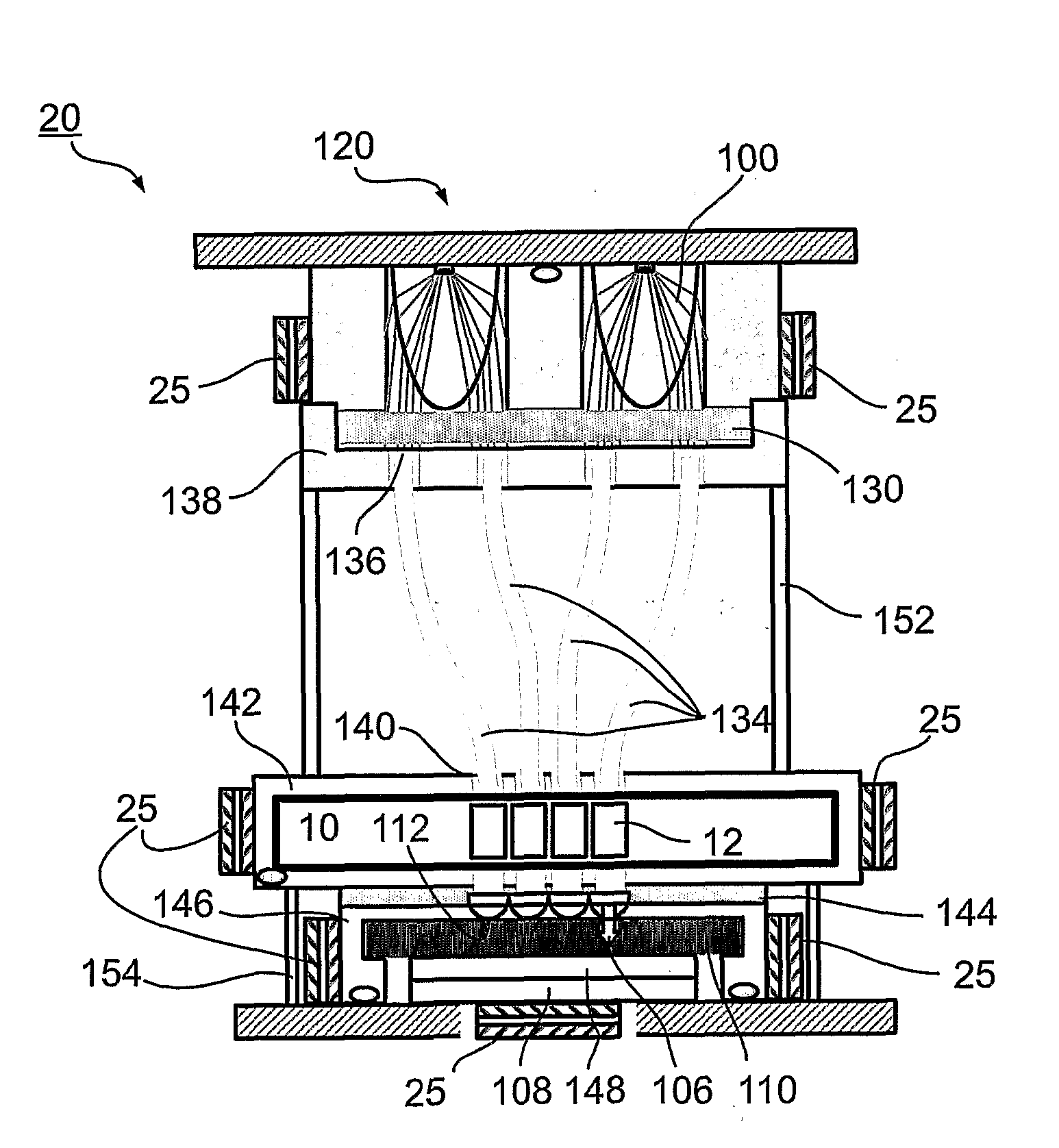
[0393]FIG. 23a illustrates reaction chamber 12, a plurality of locations 320, where biological cells generating the florescent materials are located, and a slice 322 defined in accordance with a preferred embodiment of the present invention. Reaction chamber 12 has an aperture 326 through which optical signals 106 (not shown, see FIGS. 23b-c) exit. In the following calculations, slice 322 is represented as equivalent light emitter 324, shown in FIG. 23b. Equivalent light emitter 324 is a superposition of the all the light emitter in slice 322 and can be defined, for example, by integration or summation. Also shown is excitation light 100 and optical signal 106 emitted in a plurality of directions.

[0394]FIG. 23c illustrates the spreading of optical signal 106 through aperture 326 of the reaction ch...

example 3

Sensitivity Calculation

[0417] As stated, the emission intensity is proportional to the biochemical reaction percentage expressed by the nGFP parameter. In the present example, a sensitivity calculation is performed using a signal uncertainty parameter, which is proportional to the unfiltered excitation intensity detected by the light detector:

Iunc−px=Un2B·Iexc−px·QEexc,  (EQ. 24)

where Iunc−px is the signal uncertainty parameter, Un2B is the ratio between the uncertainty to the background radiation, Iems−px is the unfiltered excitation intensity as detected by the light detector and QEexc is, as stated, the effective quantum efficiency of the detector for excitation light. A typical value for Un2B is about 0.5.

[0418] The minimal sensitivity is preferably defined such that the sensed optical signal is at least S2Un times stronger that the signal uncertainty, where S2Un is the ratio between the signal to the uncertainty:

Iems−px·QEems≧S2Un·Iunc−px,  (EQ. 25)

where Iems−px is the ...


PUM


Abstract

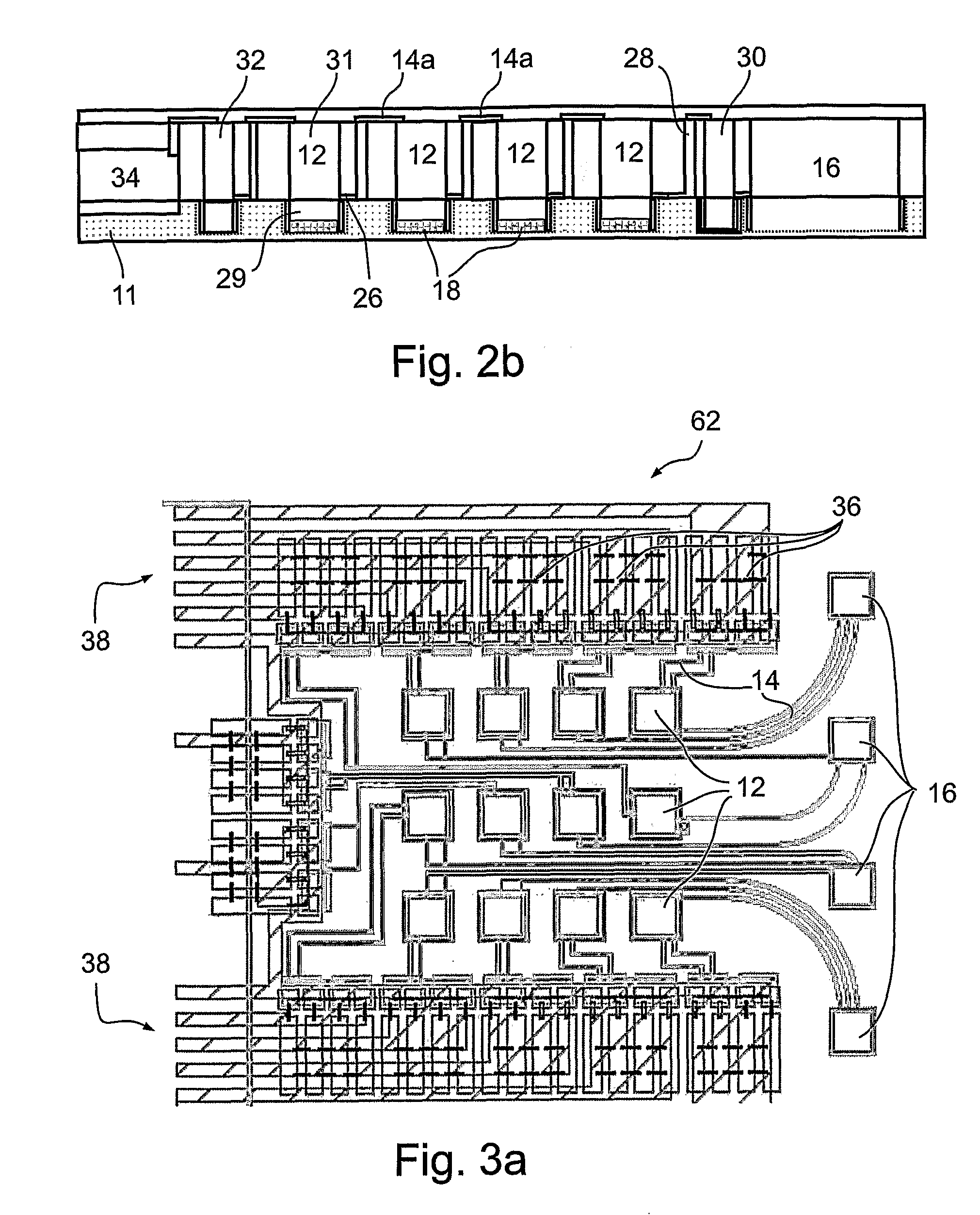
A device for detecting a presence of an analyte in a sample. The device comprises a device body configured with at least one reaction chamber configured for containing a sensor capable of producing a detectable signal when exposed to the analyte in the sample. The reaction chambers are in fluid communication with at least one sample port and at least one actuator port via a first set of microfluidic channels arranged such that application of a negative pressure to actuator port delivers fluid placed in the sample port to the reaction chambers.

Description

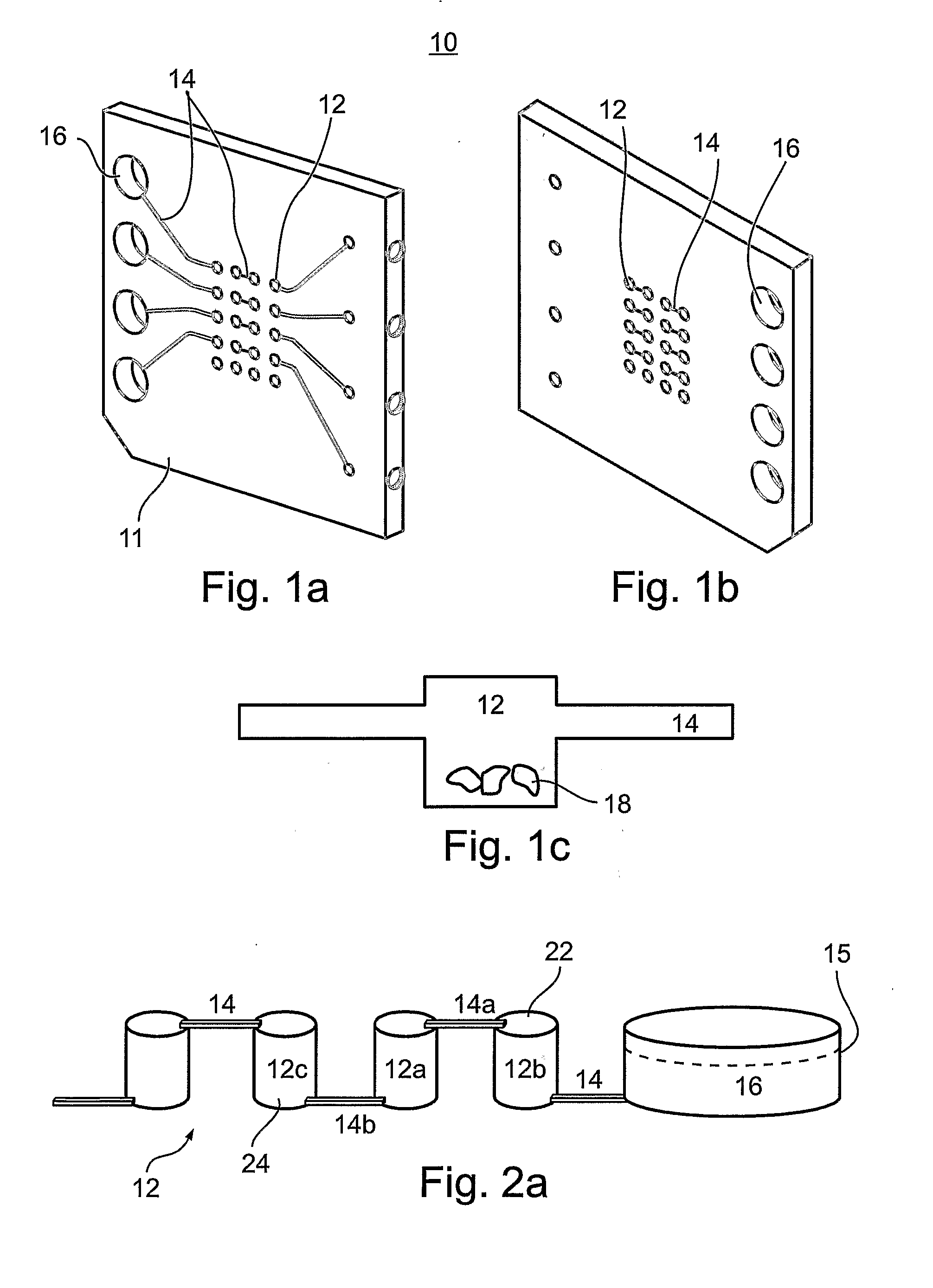
FIELD AND BACKGROUND OF THE INVENTION [0001] The present invention relates to a method and system for detecting and / or identifying analytes. In particular, the present invention relates to a device utilizing electro mechanical technology for the purpose of, for example, determining toxicity of a fluid. [0002] Much industrial and academic effort is presently directed at the development of integrated micro devices or systems combining electrical, mechanical and / or optical / electrooptical components, commonly known as Micro Electro Mechanical Systems (MEMS). MEMS are fabricated using integrated circuit batch processing techniques and can range in size from micrometers to millimeters. These systems can sense, control and actuate on the micro scale, and function individually or in arrays to generate effects on the macro scale. [0003] The development of miniaturized devices for chemical analysis and for synthesis and fluid manipulation is motivated by the prospects of improved efficiency, ...

Claims


Application Information

Patent Timeline
IPC IPC(8): C12M1/34C12Q1/00G01J1/58B01L3/00C12M1/36G01N1/10G01N21/64G01N33/487
CPCB01L3/502715B01L2200/143B01L2300/0627B01L2300/0819B01L2300/0864G01N2021/6484B01L2300/0887B01L2400/049G01N21/6452G01N2021/6482B01L2300/0874
Inventor BELKIN, SHIMSHONPEDAHZUR, RAMIROSEN, RACHELBENOVICI, ITAISHACHAM-DIAMAND, YOSIRABNER, ARTHUROKSMAN, MARK
Owner YISSUM RES DEV CO OF THE HEBREWUNIVERSITY OF JERUSALEM LTD
Why Eureka
Try Eureka