
Manufacturing method of display device

a display device and manufacturing method technology, applied in the direction of static indicating devices, discharge tubes luminescent screens, instruments, etc., can solve the problems of low thermal stability of substrates and limited process for manufacturing elements, and achieve the effects of improving productivity, high luminance, and simplifying process

Inactive Publication Date: 2007-12-06
SEMICON ENERGY LAB CO LTD
View PDF9 Cites 25 Cited by
  • Summary
  • Abstract
  • Description
  • Claims
  • Application Information

AI Technical Summary

Benefits of technology

[0009]Thus, it is an object of the present invention to provide an inorganic EL element with high luminance, which is driven over a substrate which cannot withstand high temperature such as a glass substrate. Moreover, it is another object to provide technique for manufacturing a display device which is easier and has higher productivity.
[0018]In accordance with the present invention, the first substrate and the second substrate can be separately processed. Therefore, more choices for a manufacturing method of a device are given, leading to improvement in productivity. Further, when a light-emitting material, a high dielectric material, or a conductive material is dispersed in the adhesion layer, the adhesion layer can have a function in addition to an adhering function. Accordingly, a process can be simplified.

Problems solved by technology

However, in a case where such treatment at high temperature is performed, a substrate with low thermal stability such as a glass substrate cannot be used, and accordingly, a process for manufacturing an element is limited.

Method used


Image

  • Manufacturing method of display device
  • Manufacturing method of display device
  • Manufacturing method of display device

Examples


embodiment mode 1

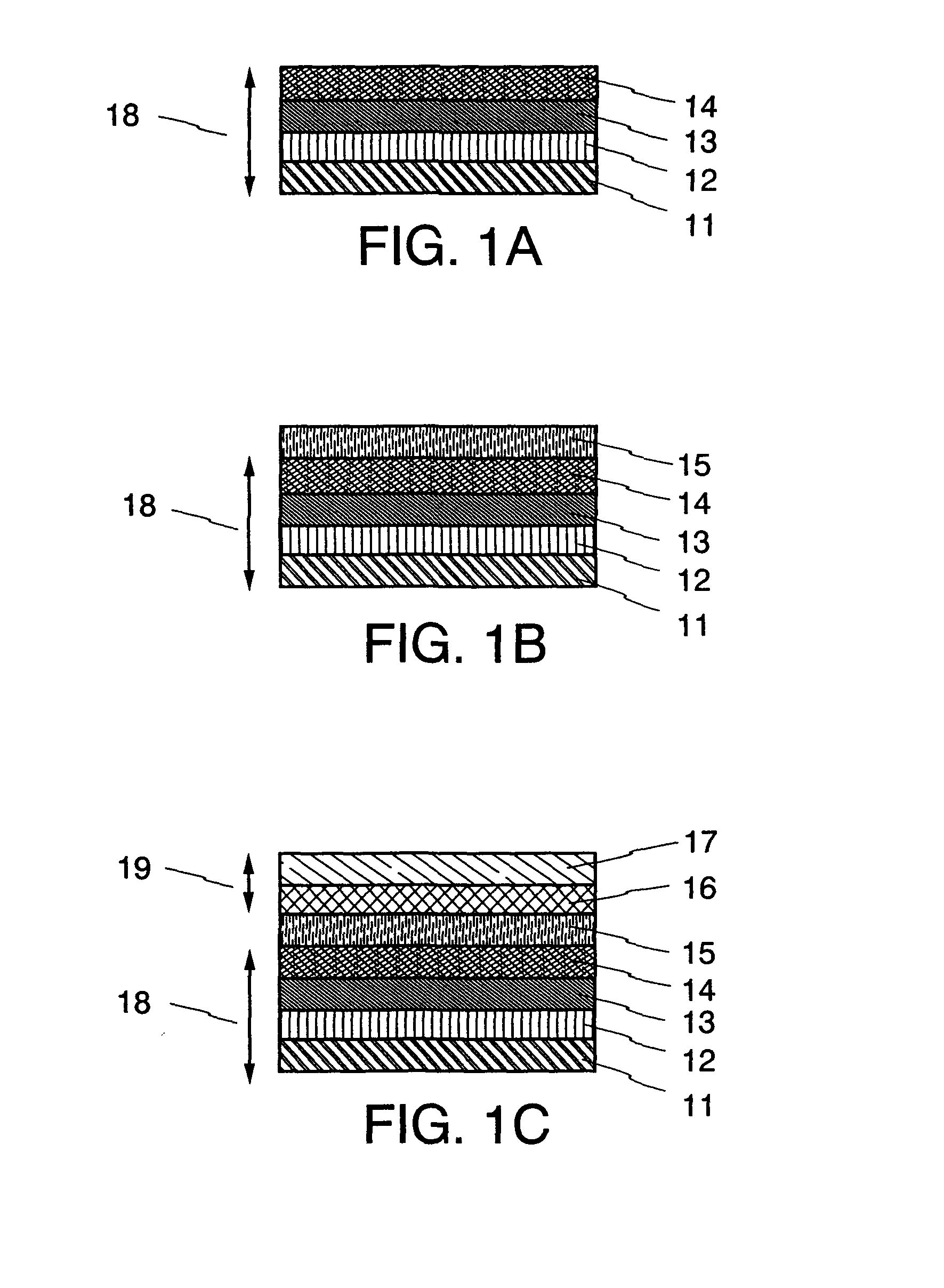
[0044]A manufacturing method of a light-emitting element in this embodiment mode will be explained in detail with reference to FIGS. 1A to 1C.

[0045]Inorganic EL elements are classified into a dispersion type inorganic EL element and a thin film type inorganic EL element depending on its element structure. They are different from each other in that the former includes a light-emitting layer in which particles of a light-emitting material are dispersed in a binder and the latter includes a light-emitting layer formed of a thin film of a fluorescent material. However, their mechanisms are common, and light emission is obtained through collision excitation of a base material or a luminescent center by electrons accelerated by a high electric field. In this embodiment mode, a manufacturing method of a thin film type inorganic EL element will be explained.

[0046]FIGS. 1A to 1C show a manufacturing method of a light-emitting element using the present invention. A structure 18 in FIG. 1A has...

embodiment mode 2

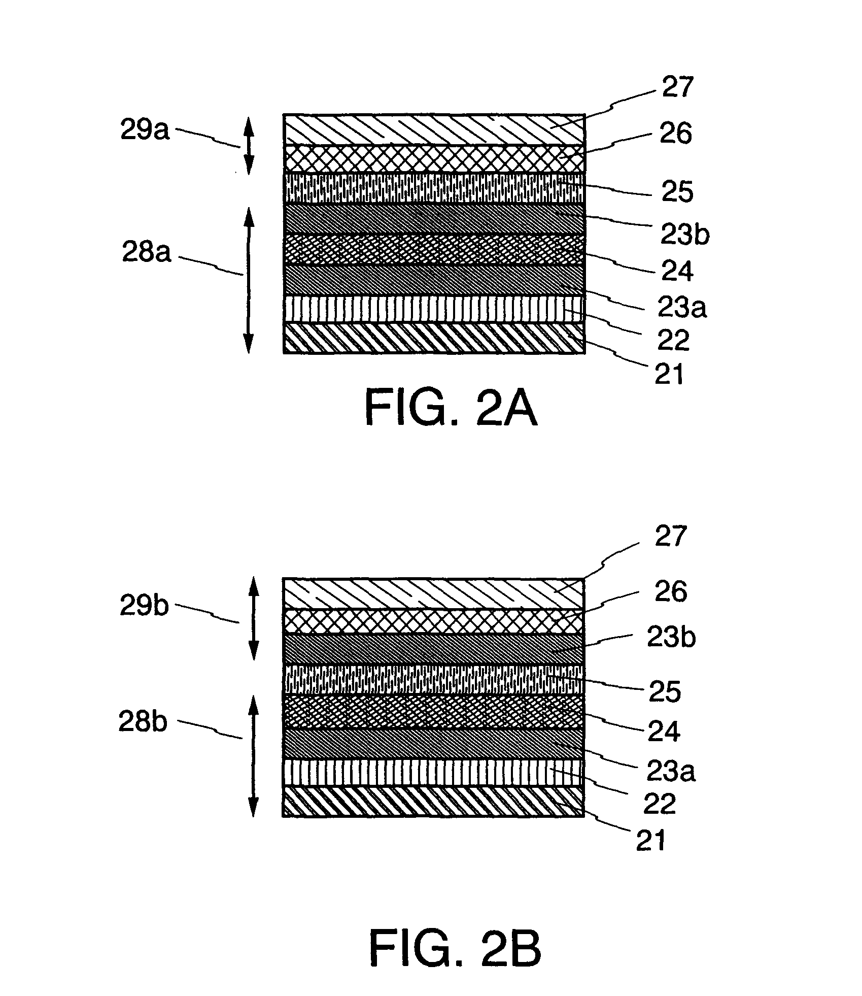
[0056]Another structural example of a light-emitting element manufactured using the present invention will be explained with reference to FIGS. 2A and 2B.

[0057]A light-emitting material that can be used for a light-emitting layer in the present invention includes a host material and an impurity element to be a light-emitting center. When the contained impurity element is changed, various color emission can be obtained. As a manufacturing method of a light-emitting material, various methods such as a solid phase method and a liquid phase method (a coprecipitation method) can be used. Alternatively, a spraying thermal decomposition method, a double decomposition method, a method by thermal decomposition reaction of a precursor, a reversed micelle method, a method in which these methods and high temperature baking are combined, a liquid phase method such as a freeze-drying method, or the like can be used.

[0058]The solid phase method is a method in which a host material and an impurity ...

embodiment mode 3

[0076]A light-emitting element which can be manufactured using the present invention will be explained with reference to FIGS. 3A to 3C. In this embodiment mode, a manufacturing method of a dispersion type inorganic EL element will be explained.

[0077]A structure 30 in FIG. 3A is a structure having a first substrate 31 and a first electrode 32.

[0078]An object in which a light-emitting material 33 is dispersed in an adhesion resin 34 is attached over the first electrode 32 of the structure 30 to form an adhesion layer 40a.

[0079]As the light-emitting material 33 herein used, the light-emitting material shown in Embodiment Mode 2 is processed into particles. The light-emitting material may be processed by being crushed in a mortar or the like, or through the use of a device such as a mill. When a particle having a sufficiently desired size can be obtained by a manufacturing method of the light-emitting material, further processing may not be performed. The particle diameter may be grea...


PUM


Abstract

A first light-transmitting substrate having a first light-transmitting electrode layer and a second substrate having at least a second electrode layer are attached to each other with a resin which is cured by UV light or the like, to form an inorganic EL light-emitting element. Thus, a display device is manufactured. The light-emitting layer may be interposed between the first light-transmitting substrate having the first electrode layer and the second substrate having the second electrode layer, and may be formed either on the first electrode layer side or on the second electrode layer side.

Description

BACKGROUND OF THE INVENTION[0001]1. Field of the Invention[0002]The present invention relates to a manufacturing method of a display device.[0003]2. Description of the Related Art[0004]In recent years, a liquid crystal display device and an electroluminescence display device, in which thin film transistors (hereinafter also referred to as TFTs) are formed over a glass substrate in an integrated manner, have been developed. In each of these display devices, a thin film transistor is formed over a glass substrate by using technique for forming a thin film, and a liquid crystal element or a light-emitting element (an electroluminescence element, hereinafter also referred to as an EL element) is formed as a display element over various circuits composed of the thin film transistors so that the device functions as a display device.[0005]Light-emitting elements utilizing electroluminescence are classified depending on whether a light-emitting material is an organic compound or an inorgani...

Claims


Application Information

Patent Timeline
Patent Type & Authority Applications(United States)
IPC IPC(8): H01L21/00
CPCG09G3/3225H01J1/66H01J1/64G09G5/363H05B33/10H05B33/22
Inventor IBE, TAKAHIROSATO, YOSUKE
Owner SEMICON ENERGY LAB CO LTD
Learn More