Chemical vapor deposition of high quality flow-like silicon dioxide using a silicon containing precursor and atomic oxygen

a technology of flow-like silicon and chemical vapor deposition, which is applied in chemical vapor deposition coating, coating, metallic material coating process, etc., can solve the problems of difficult to completely fill gaps and trenches in these structures without creating, and the difficulty of electrical noise too large,

Active Publication Date: 2007-12-06
APPLIED MATERIALS INC
View PDF99 Cites 451 Cited by
  • Summary
  • Abstract
  • Description
  • Claims
  • Application Information

AI Technical Summary

Benefits of technology

[0012] Additional embodiments and features are set forth in part in the description that follows, and in part will become apparent to those skilled in the art upon examination of the specification or may be learned by the practice of the invention. The features and advantages of the invention may be realized and attained by means of the instrumentalities, combinations, and methods described in the specification.

Problems solved by technology

While the ability to make device structures with ever increasing aspect ratios has allowed more of the structures (e.g., transistors, capacitors, diodes, etc.) to be packed onto the same surface area of a semiconductor chip substrate, it has also created fabrication problems.
Once of these problems is the difficulty of completely filling the gaps and trenches in these structures without creating a void or seam during the filling process.
If the gaps were left empty, there would be too much electrical noise, and current leakage for the devices to operate properly (or at all).
As aspect ratios increased however, it became more difficult to fill the deep, narrow trench without having a blockage start a void or seam in the fill volume.
Voids and seams in a dielectric layer cause create problems both during semiconductor device fabrication and in the finished devices.
This results in unpredictable and inconsistent post-deposition processing of the layer, such as even etching, polishing, annealing, etc.
This can result in uneven, and inferior device performance due to electrical crosstalk, charge leakage, and even shorting within and between device elements.
Unfortunately however, slowing the deposition rate means increasing the deposition time, which reduces processing efficiency and production rates.
Unfortunately however, increasing the moisture level during a silicon oxide deposition can also adversely effect the properties of the deposited film, including its density (i.e., an increased wet etch rate ratio (WERR)) and dielectric properties (i.e., an increased k-value).

Method used


Image

  • Chemical vapor deposition of high quality flow-like silicon dioxide using a silicon containing precursor and atomic oxygen
  • Chemical vapor deposition of high quality flow-like silicon dioxide using a silicon containing precursor and atomic oxygen
  • Chemical vapor deposition of high quality flow-like silicon dioxide using a silicon containing precursor and atomic oxygen

Examples


Embodiment Construction

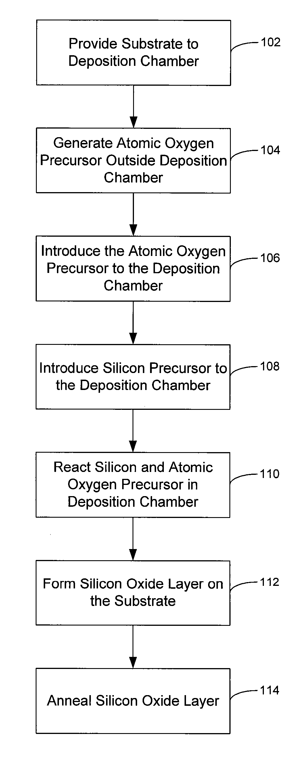
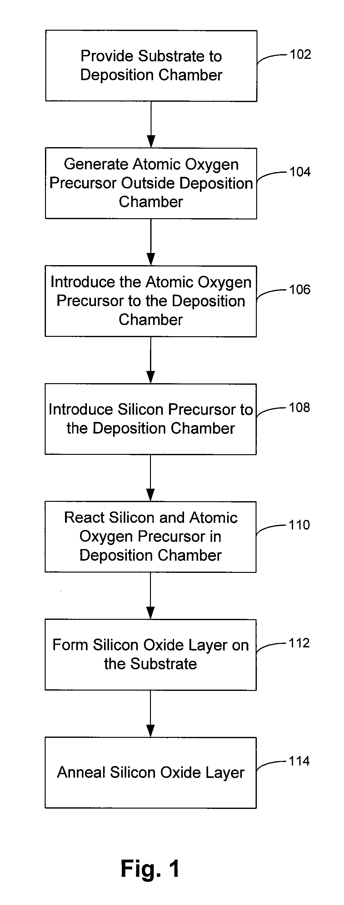
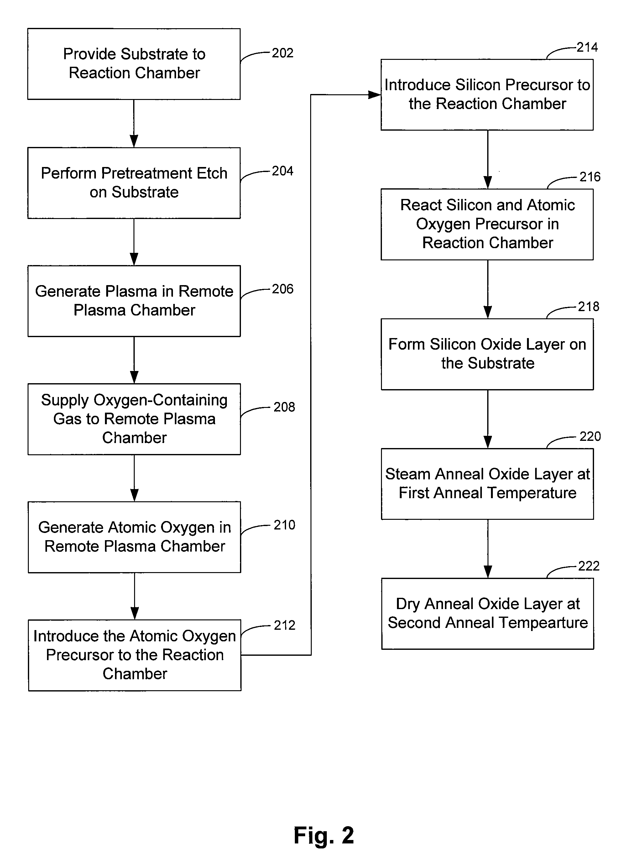
[0021] Systems and methods are described for depositing a silicon oxide layer with high flowability that is then cured (i.e., annealed) into a high-quality oxide layer or fill. The high flowability of the initially formed oxide allows it to fill high aspect ratio gaps and trenches (e.g., aspect ratios greater than 5:1) without gaps or seams. The curing step then drives out moisture to leave behind a dense oxide film having a wet etch rate ratio (WERR) that may approach the practical limit for silicon oxide films (e.g., WERRs down to about 1.8 to about 1.4). For films made with carbon containing silicon precursors, low-k oxide films may be produced that also have high initial flowability and high post-cure quality.

[0022] The methods of the invention include the remote generation of reactive atomic oxygen outside a deposition / reaction chamber. The atomic oxygen is first mixed with a silicon precursor in the deposition chamber, where they quickly react even at low temperatures and pre...


PUM

PropertyMeasurementUnit
diameteraaaaaaaaaa
temperatureaaaaaaaaaa
pressureaaaaaaaaaa

Abstract

Methods of depositing a silicon oxide layer on a substrate are described. The methods may include the steps of providing a substrate to a deposition chamber, generating an atomic oxygen precursor outside the deposition chamber, and introducing the atomic oxygen precursor into the chamber. The methods may also include introducing a silicon precursor to the deposition chamber, where the silicon precursor and the atomic oxygen precursor are first mixed in the chamber. The silicon precursor and the atomic oxygen precursor react to form the silicon oxide layer on the substrate, and the deposited silicon oxide layer may be annealed. Systems to deposit a silicon oxide layer on a substrate are also described.

Description

CROSS-REFERENCES TO RELATED APPLICATIONS [0001] This application claims the benefit of U.S. Provisional Application No. 60 / 803,483 by Ingle et al, filed May 30, 2006 and titled “CHEMICAL VAPOR DEPOSITION OF HIGH QUALITY FLOW-LIKE SILICON DIOXIDE USING A SILICON CONTAINING PRECURSOR AND ATOMIC OXYGEN”. This application is also related to co-assigned U.S. Provisional App. No. 60 / 803,489, by Munro et al, filed May 30, 2006 and titled “A METHOD FOR DEPOSITING AND CURING LOW-K FILMS FOR GAPFILL AND CONFORMAL FILM APPLICATIONS”. This application is also related to U.S. Provisional Application No. 60 / 803,481, by Chen et al, filed May 30, 2006 and titled “A NOVEL DEPOSITION-PLASMA CURE CYCLE PROCESS TO ENHANCE FILM QUALITY OF SILICON DIOXIDE”. In addition, this application is related to U.S. Provisional Application No. 60 / 803,499 by Lubomirsky, filed May 30, 2006 and titled “PROCESS CHAMBER FOR DIELECTRIC GAPFILL”. The entire contents of the priority U.S. Provisional patent application and ...

Claims


Application Information

Patent Timeline
Patent Type & Authority Applications(United States)
IPC IPC(8): H01L21/31
CPCC23C16/401C23C16/452C23C16/56H01L21/31612H01L21/02274H01L21/02337H01L21/02164C23C16/402H01L21/3105H01L21/02315H01L21/31H01L21/02126H01L21/02216
Inventor INGLE, NITIN K.YUAN, ZHENGGEE, PAULSAPRE, KEDAR
Owner APPLIED MATERIALS INC
Why Eureka
Try Eureka