

Precursor Film And Method Of Forming The Same
- Summary
- Abstract
- Description
- Claims
- Application Information
AI Technical Summary
Benefits of technology
Problems solved by technology
Method used
Image

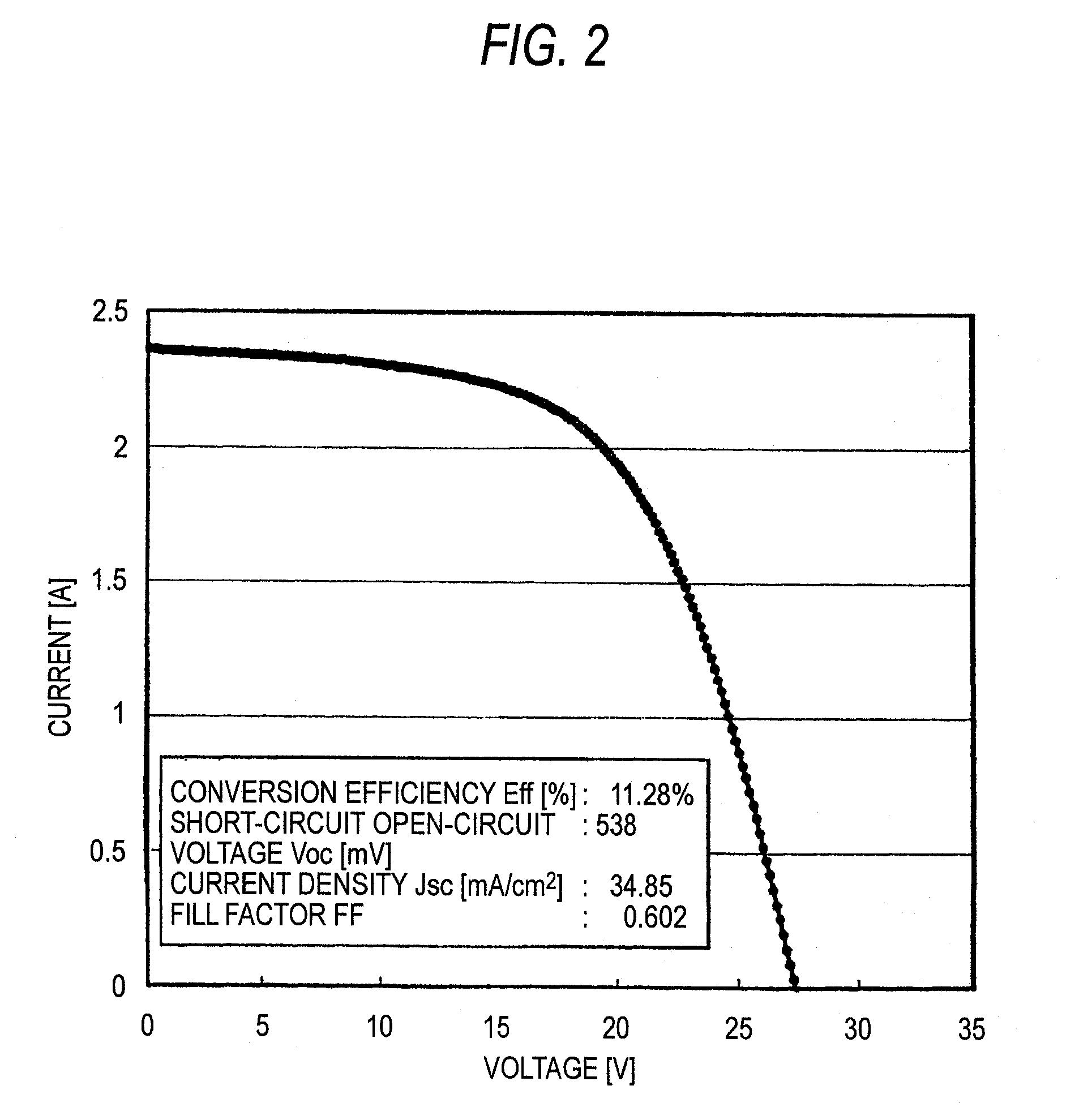
Examples
Embodiment Construction
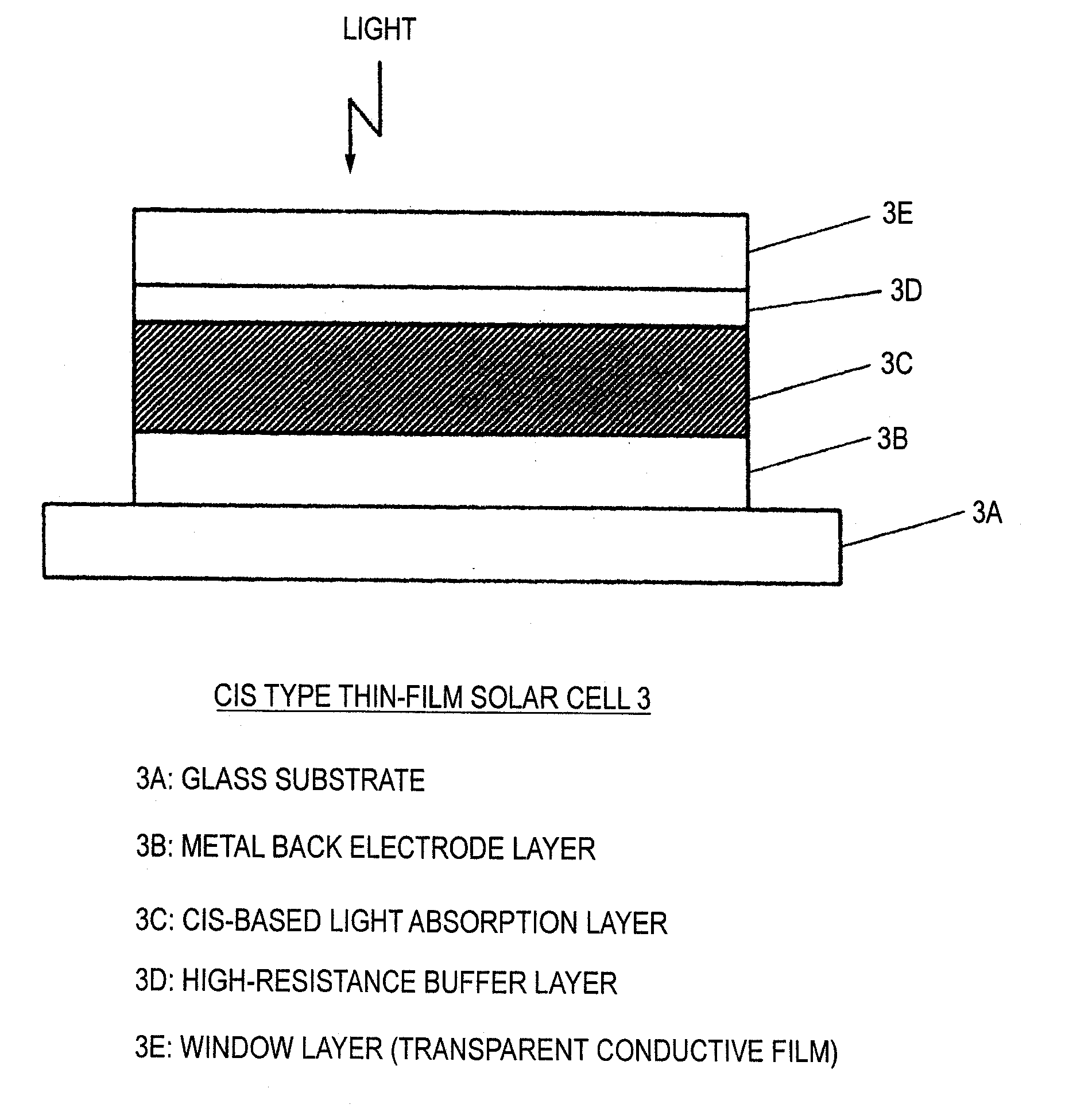
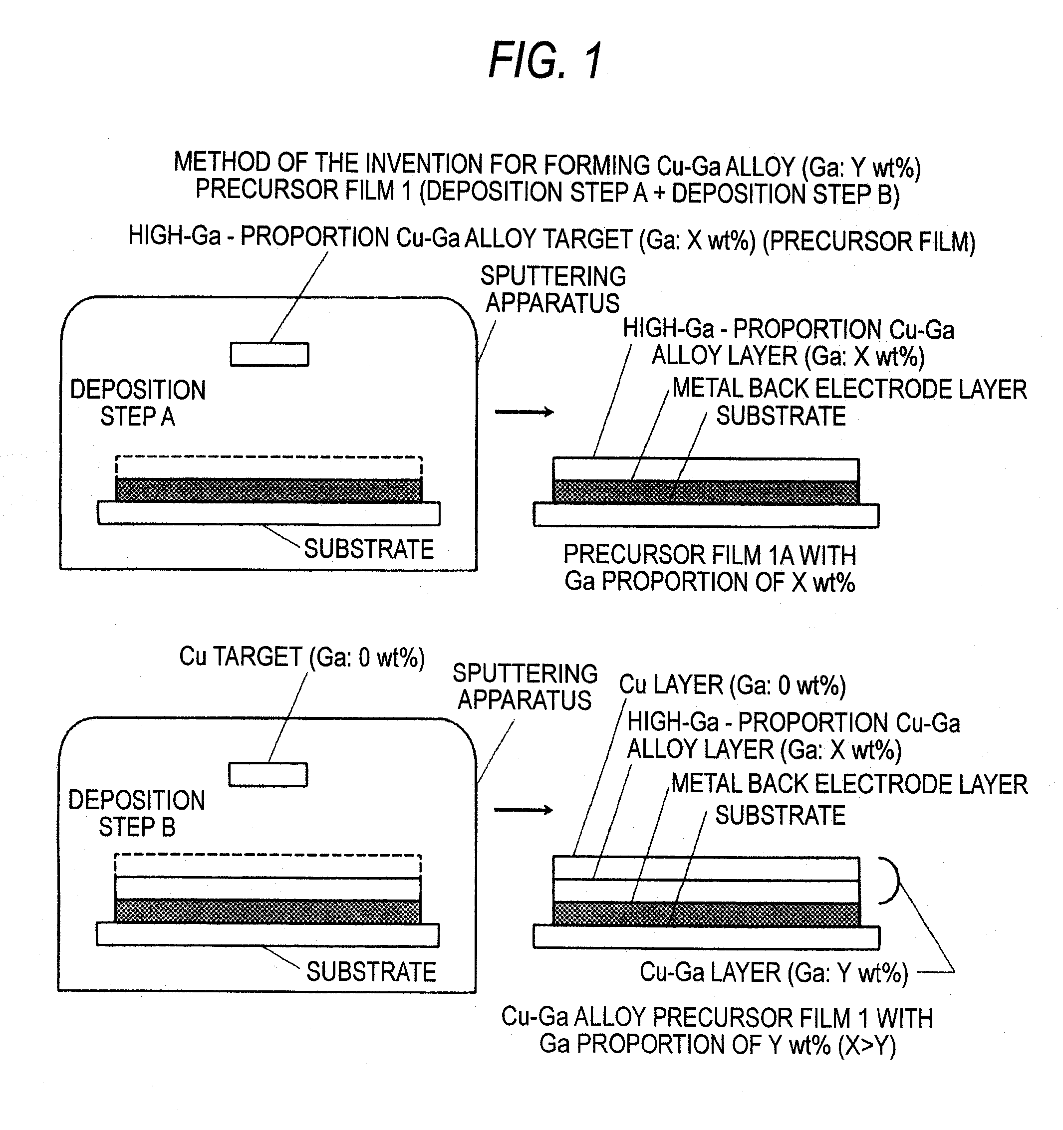
[0016] The invention relates to a method of forming a Cu—Ga precursor film for use in forming the light absorption layer of a CIS type thin-film solar cell which contains copper, indium, gallium, sulfur, and selenium among the components thereof, such as CISS or CIGSSe. The invention provides a precursor film for use in the step of forming the light absorption layer of a CIS type thin-film solar cell which is a pn heterojunction device having a substrate structure comprising a glass substrate, a metal back electrode layer, a CIS-based light absorption layer, a high-resistance buffer layer, and an n-type window layer which have been superposed in this order as shown in FIG. 6. The invention further provides a method of forming the film.
[0017] The CIS-based light absorption layer comprises, e.g., p-type CGS, CGSSe, CIGS, or CIGSSe, which each contain copper and gallium. The CIGS, CIGSSe, and the like contain copper, indium, gallium, sulfur, and selenium among the components thereof. ...
PUM
| Property | Measurement | Unit |
|---|---|---|
| Weight | aaaaa | aaaaa |
| Electrical resistance | aaaaa | aaaaa |
| Light | aaaaa | aaaaa |
Abstract
Description
Claims
Application Information