Resonating conductive traces and methods of using same for bonding components

Inactive Publication Date: 2007-12-13
LAMBDA TECH
View PDF1 Cites 27 Cited by
  • Summary
  • Abstract
  • Description
  • Claims
  • Application Information

AI Technical Summary

Benefits of technology

[0030] According to other embodiments of the present invention, flat substrates can be sealed at their perimeters, for example, in MEMS applications where a glass plate is sealed at the perimeter with an

Problems solved by technology
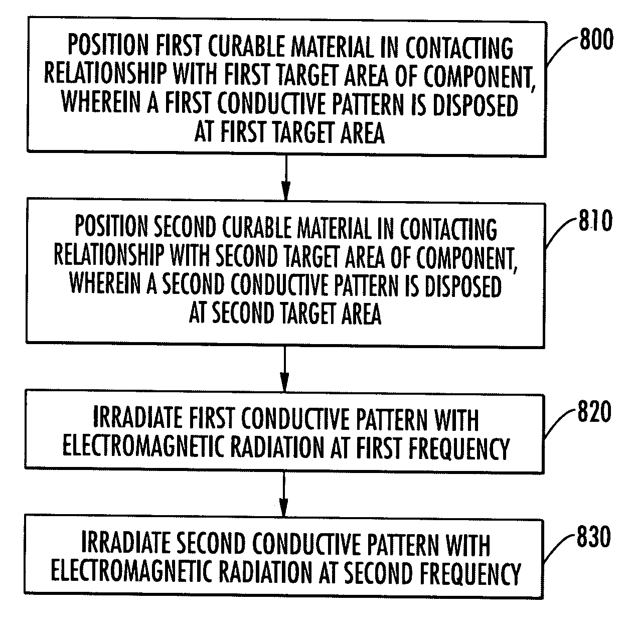
Unfortunately, there are drawbacks associated with these conventional methods.
For example, encapsulation with a liquid dielectric material typically results in excess dielectric material which must be properly disposed of.
In addition, the electrical performance of microelectronic components encapsulated in dielectric material can suffer.
This is because the encapsulating dielectric material that surrounds the electrical leads of a microelectronic component can induce low signal propagation speeds.
In fact, the higher the dielectric constant of the dielectric material surrounding the electrical leads, the slower the propagation speed of electrical signals.
Another problem is that encapsulating material and electronic components encapsulated therein can have mismatched coefficients of thermal expansion, which can result in harmful stresses in some temperature environments.
Ultrasonic welding can be limited in performance when two dissimilar materials (e.g., materials having dissimilar elastic modulus or other properties) are to be joined together.
In addition, it can be difficult to apply uniform cyclic mechanical forces to the structures having multiple walls and/or complex shapes as is often encountered in microelectronics packaging.
As such, accurate alignment can be d

Method used


Image

  • Resonating conductive traces and methods of using same for bonding components
  • Resonating conductive traces and methods of using same for bonding components
  • Resonating conductive traces and methods of using same for bonding components

Examples


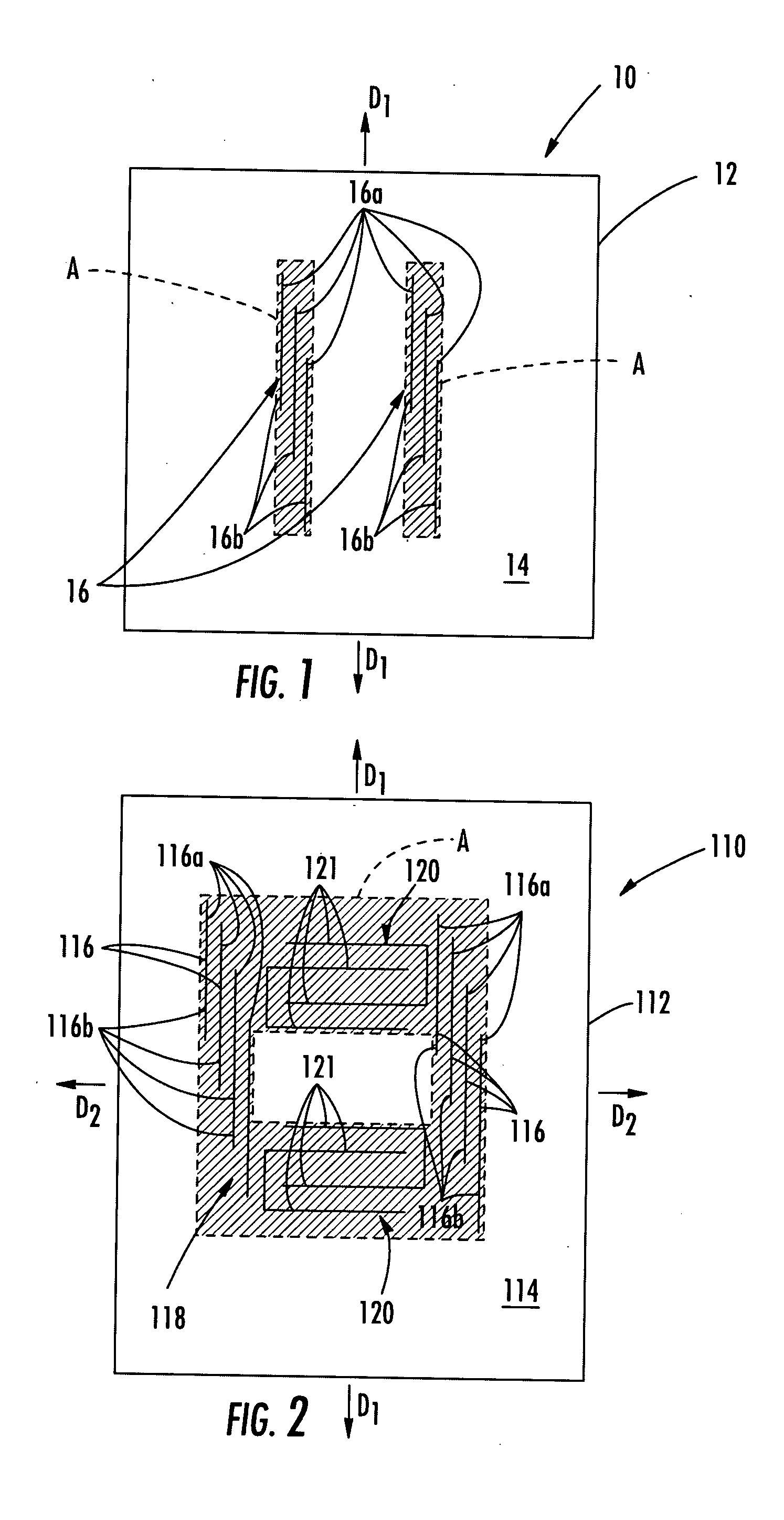
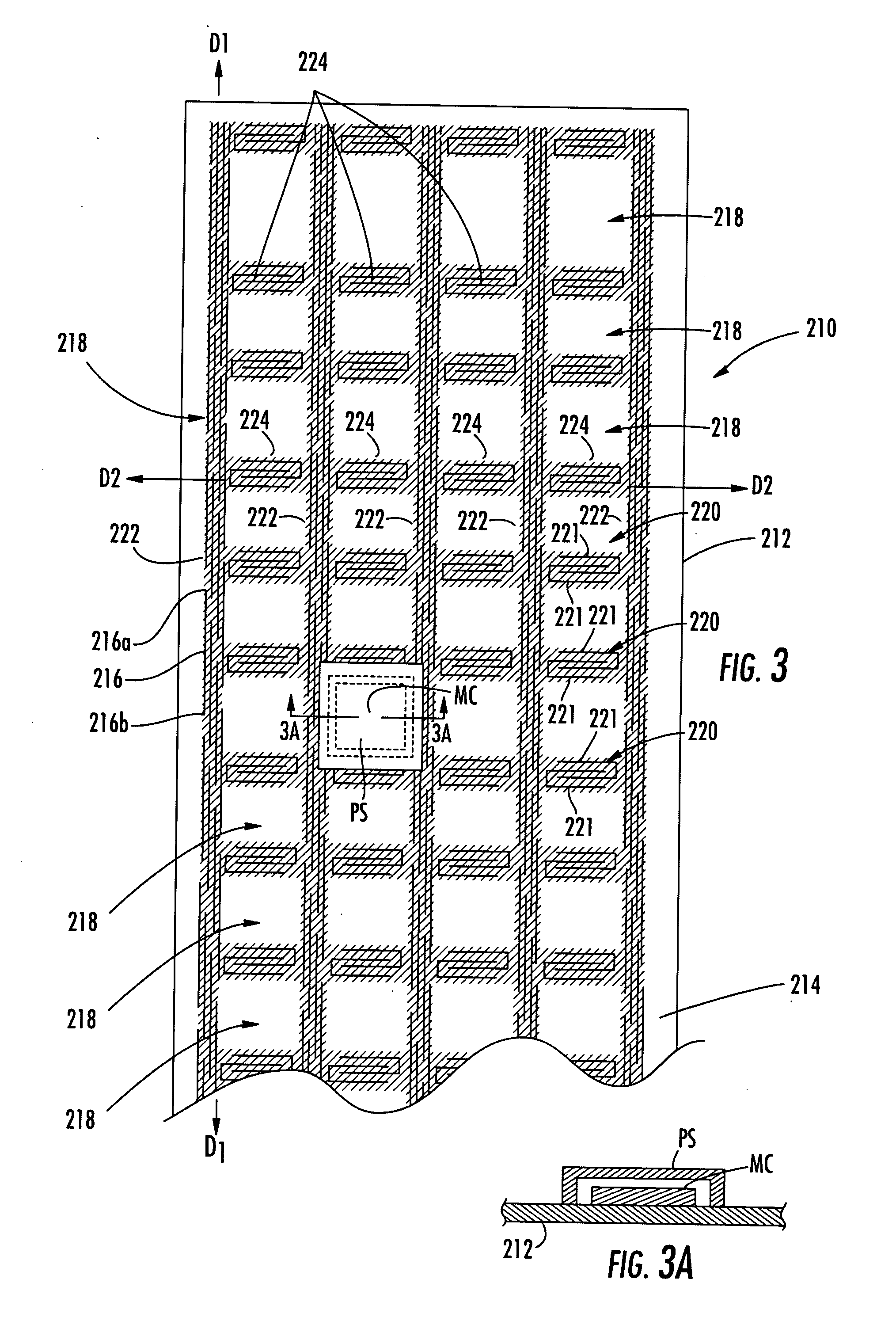
Embodiment Construction

[0038] While the invention is susceptible to various modifications and alternative forms, specific embodiments thereof are shown by way of example in the drawings and will herein be described in detail. It should be understood, however, that there is no intent to limit the invention to the particular forms disclosed, but on the contrary, the invention is to cover all modifications, equivalents, and alternatives falling within the spirit and scope of the invention as defined by the claims. Like reference numbers signify like elements throughout the description of the figures.

[0039] As used herein, the singular forms “a,”“an,” and “the” are intended to include the plural forms as well, unless expressly stated otherwise. It should be further understood that the terms “comprises” and / or “comprising” when used in this specification are taken to specify the presence of stated features, integers, steps, operations, elements, and / or components, but do not preclude the presence or addition ...


PUM

PropertyMeasurementUnit
Temperatureaaaaaaaaaa
Lengthaaaaaaaaaa
Angleaaaaaaaaaa

Abstract

Conductive traces and patterns of same are used to bond components together via electromagnetic radiation. Each conductive trace is configured to resonate and heat up when irradiated with electromagnetic radiation, such as microwave energy and/or RF energy, having a wavelength that is about 2.3 times the length of the conductive trace. The conductive traces may be arranged in a pattern to uniformly heat a target area of a substrate or other component to a selected temperature when irradiated with electromagnetic radiation.

Description

RELATED APPLICATION [0001] This application claims the benefit of and priority to U.S. Provisional Patent Application No. 60 / 809,435, filed May 30, 2006, the disclosure of which is incorporated herein by reference as if set forth in its entirety.FIELD OF THE INVENTION [0002] The present invention relates generally to bonding components together, and more particularly to bonding components with electromagnetic radiation. BACKGROUND OF THE INVENTION [0003] It may be desirable to seal microelectronic components, such as semiconductor devices and integrated circuits (ICs), attached to printed circuit boards (PCBs) and other articles. Sealing a microelectronic component attached to a PCB can be accomplished using a variety of known methods including, for example, enclosing the microelectronic component within a physical enclosure and then sealing the enclosure, or encapsulating the microelectronic component with a liquid dielectric material that is subsequently solidified. [0004] Unfortu...

Claims


Application Information

Patent Timeline
IPC IPC(8): B29C65/48H05B6/64H05K1/00
CPCB29C65/04B29C65/4865B29C65/1425B29C65/4835B29C66/20B29C66/54B29K2995/0006B29L2031/30B29L2031/3061B29L2031/3425B29L2031/3475B29L2031/50H01L24/29H01L24/32H01L24/83H01L2224/83234H01L2224/83855H01L2224/8388H01L2924/01005H01L2924/01013H01L2924/01015H01L2924/01029H01L2924/01038H01L2924/01047H01L2924/01082H01L2924/07802H01L2924/09701H01L2924/14H05K3/3494H05K2201/0394H05K2203/102B29C65/1406B29C66/964H01L2924/00013H01L2224/293H01L2224/2929H01L2924/0665H01L2924/01033H01L2924/01006H01L2224/2919H01L2224/29B29C65/366B29C65/1403B29C65/00H01L2924/00014H01L2924/00H01L2224/29099H01L2224/29199H01L2224/29299B29C66/73112B29C66/73921H01L2224/8322H01L2224/83862H01L2924/351
Inventor FATHI, ZAKARYAEGREATHOUSE, STEVEHUBBARD, ROBERTAHMAD, IFTIKHAR
Owner LAMBDA TECH
Why Eureka
Try Eureka