Low power and low pin count bi-directional dual data rate device interconnect interface

Active Publication Date: 2007-12-13
MICROCHIP TECH INC
View PDF18 Cites 6 Cited by
  • Summary
  • Abstract
  • Description
  • Claims
  • Application Information

AI Technical Summary

Benefits of technology

[0025]In general, various embodiments of the invention may combine a simple clock source synchronous DDR data transfer mechanism with static bus state signaling to replace a complex bus like USB with an easy to implement digital serial interconnect bus. This may eliminate the various pull-up and pull-down resistors required in USB, and enable the interconnect bus to operate with little or no leakage current when the bus is in an idle state, or data transmission state. All of the required functionality may be implemen

Problems solved by technology

However, standard USB devices include an analog physical layer (PHY) component, along with pull-up and pull-down resistors that constantly consume power (even when in suspend or standby).
These aspects of USB make it less attractive to power conscious embedded devices, particularly those operating from a battery.
The USB-IF (USB Implementers Forum) created and released an Interchip 1.0 specification addressing some of the analog PHY issues of USB, and is therefore more attractive for portable devices, but the interface is not capable of HS (high speed) USB transfer speeds, and retains the differential data (D+/D−) aspect of USB, which typically requires eye diagrams, clock recovery and synchronization.
This increases the complexity of the implementation over a straightforward digital clock and data interface, and limits the transmission length to 10 cm or less.
It also makes it ve

Method used


Image

  • Low power and low pin count bi-directional dual data rate device interconnect interface
  • Low power and low pin count bi-directional dual data rate device interconnect interface

Examples


Example

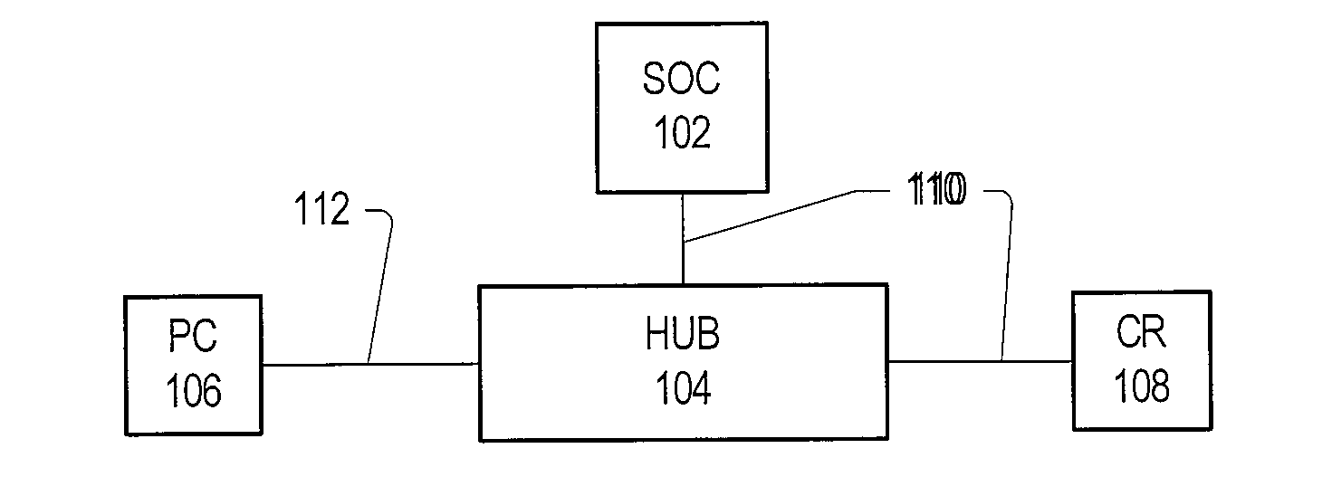
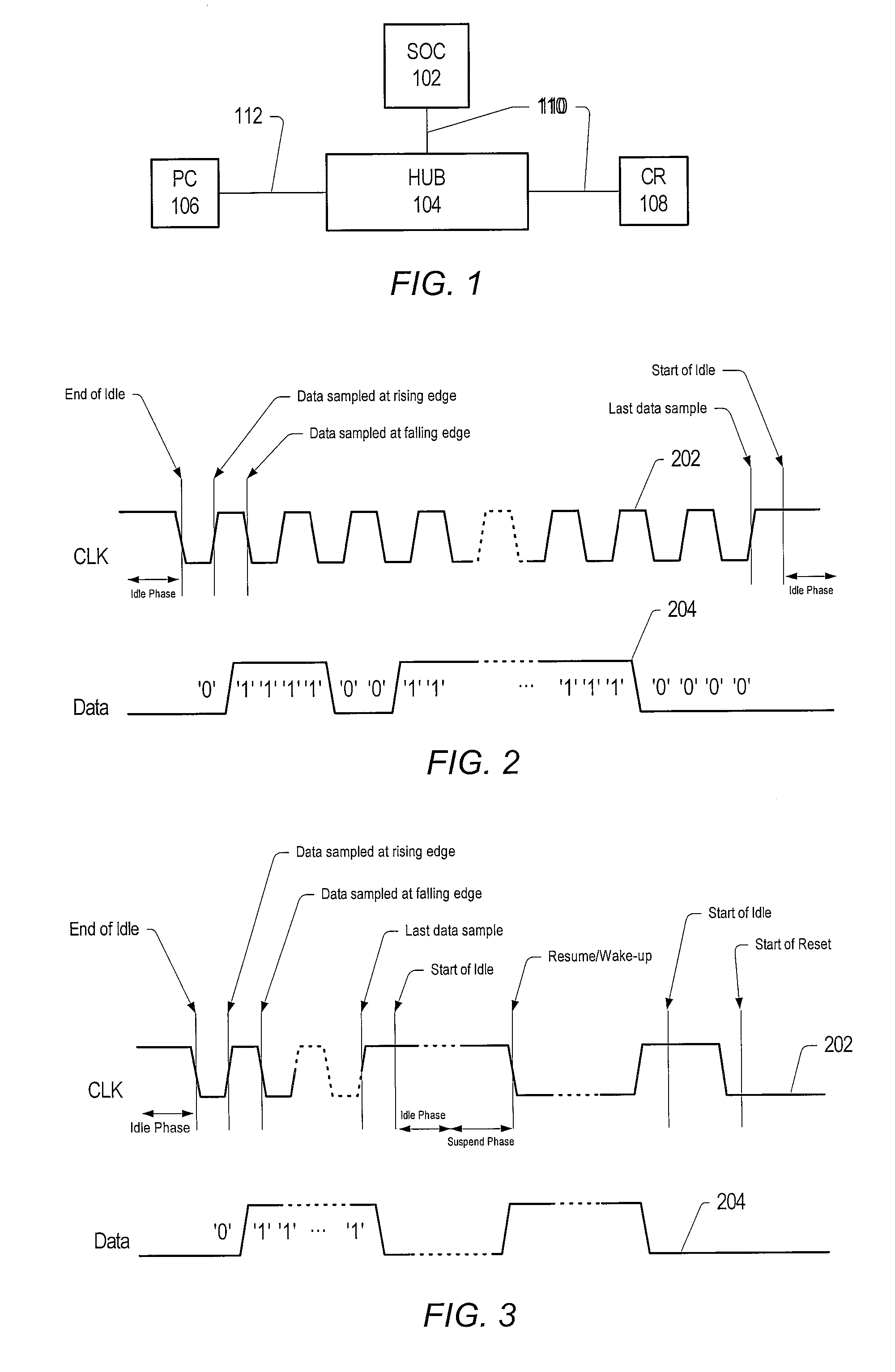
[0031]In one set of embodiments, a 2-wire (or at least 2-wire) digital bus may be configured to interconnect USB devices and controllers without using a USB physical layer (PHY) or USB cable. One wire may be a bidirectional clock (CLK) line / signal and the other wire may be a bidirectional data line / signal. In certain embodiments, the clock signal may only be active during a data transfer, and data may be clocked on rising and falling edges of the clock, thereby implementing a double data rate (DDR) transfer protocol. The transmitting device may source the CLK signal simultaneously and synchronously with the data, while the receiving device may clock the data during transitions of the clock line. In one embodiment, the bus may comprise one or more double data rate (DDR) data lines, which may all be source synchronous with the CLK line. Voltage levels may be process / device specific. FIG. 1 illustrates a block diagram of an exemplary system in which a 2-wire bidirectional bimodal bus 1...


PUM


Abstract

A simple clock source synchronous DDR data transfer mechanism may be combined with static bus state signaling to replace a complex bus (e.g. USB) with an easy to implement digital serial interconnect bus. This may eliminate various pull-up/pull-down resistors required in USB, and enable the interconnect bus to operate with little or no leakage current when the bus is in an idle state, or data transmission state. All required functionality may be implemented using only two signal pins. The interconnect bus may also enable silicon solutions for high speed USB that do not require a PLL, since the clock may be provided by the transmission source and may thus not need to be recovered from the serial data stream. The digital serial interconnect bus may provide an easy reuse mechanism for USB silicon by enabling a designer to remove the analog PHY and replace it with a serial digital I/O transfer mechanism, while retaining the IP's USB timers, and other protocol specific features.

Description

PRIORITY CLAIM[0001]This application claims benefit of priority of provisional application Ser. No. 60 / 804,141 titled “Low Power and Low Pin Count Bi-Directional Dual Data Rate Device Interconnect Interface”, filed on Jun. 7, 2006, whose inventor is Mark. R. Bohm, and which is hereby incorporated by reference as though fully and completely set forth herein.BACKGROUND OF THE INVENTION[0002]1. Field of the Invention[0003]The present invention relates generally to digital device interfaces, and more specifically to low pin count interfaces to interconnect USB devices on a circuit board.[0004]2. Description of the Related Art[0005]The Universal Serial Bus (USB) allows coupling of peripheral devices to a computer system. USB is a serial cable bus for data exchange between a host computer and a wide range of simultaneously accessible devices. The bus allows peripherals to be attached, configured, used, and detached while the host is in operation. For example, USB printers, scanners, digit...

Claims


Application Information

Patent Timeline
IPC IPC(8): G06F13/42
CPCG06F1/3203G06F1/3253Y02B60/1235G06F2213/0042G06F13/4291Y02D10/00G06F13/00G06F13/14G06F13/42
Inventor BOHM, MARK R.
Owner MICROCHIP TECH INC
Why Eureka
Try Eureka