Power Semiconductor Module and Fabrication Method Thereof
a technology of power semiconductor modules and fabrication methods, which is applied in the direction of printed circuit stress/warp reduction, printed circuit aspects, stacked spaced pcbs, etc., can solve the problems of power module airtightness loss and inside contamination, and achieve high reliability, prevent the degrade of voltage resistance of power semiconductor modules, and high reliability
- Summary
- Abstract
- Description
- Claims
- Application Information
AI Technical Summary
Benefits of technology
Problems solved by technology
Method used
Image

Examples
first embodiment
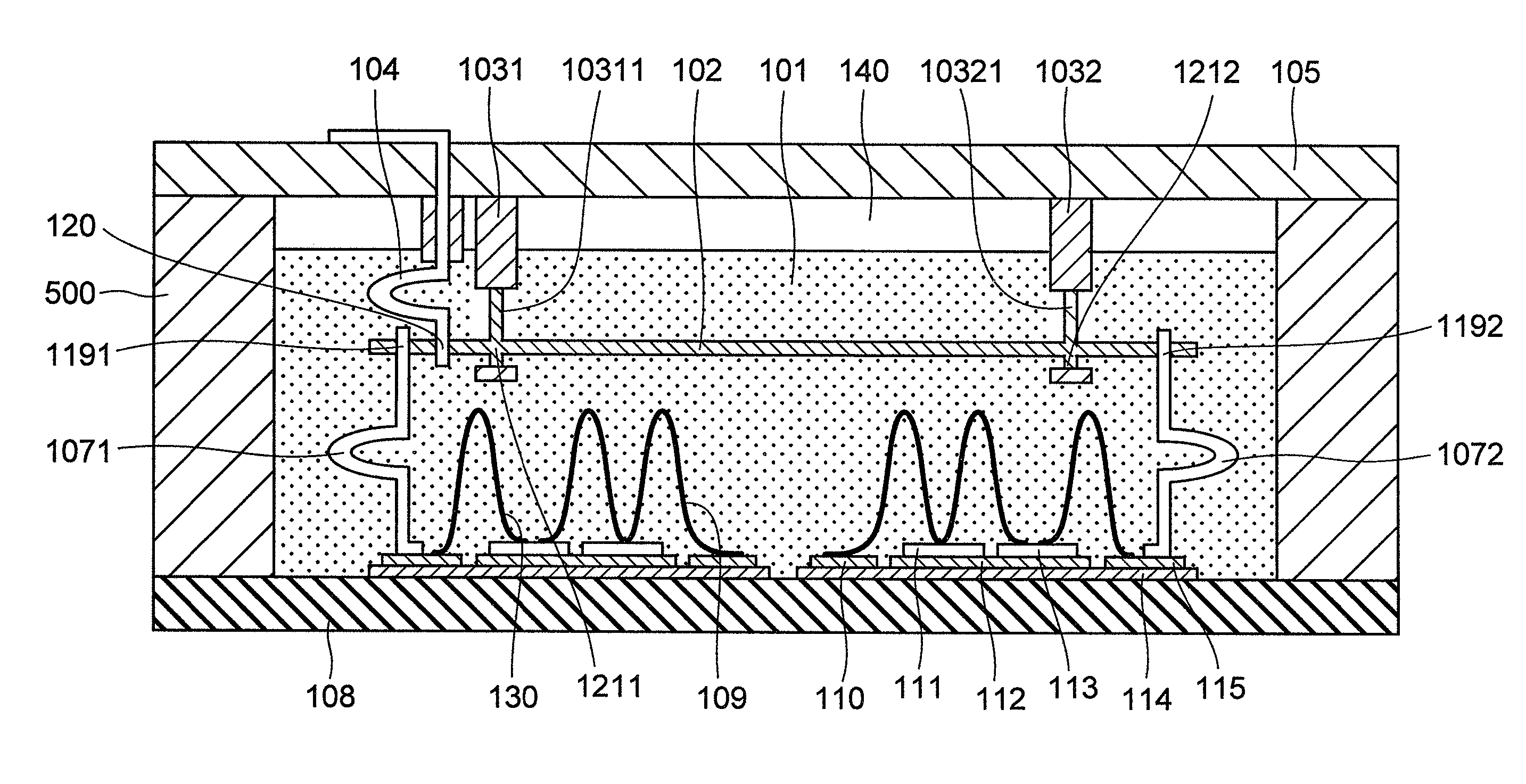
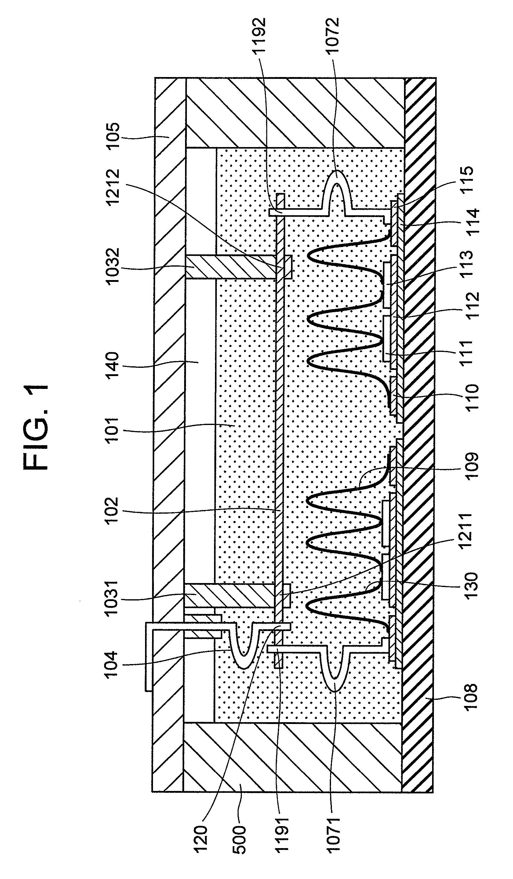
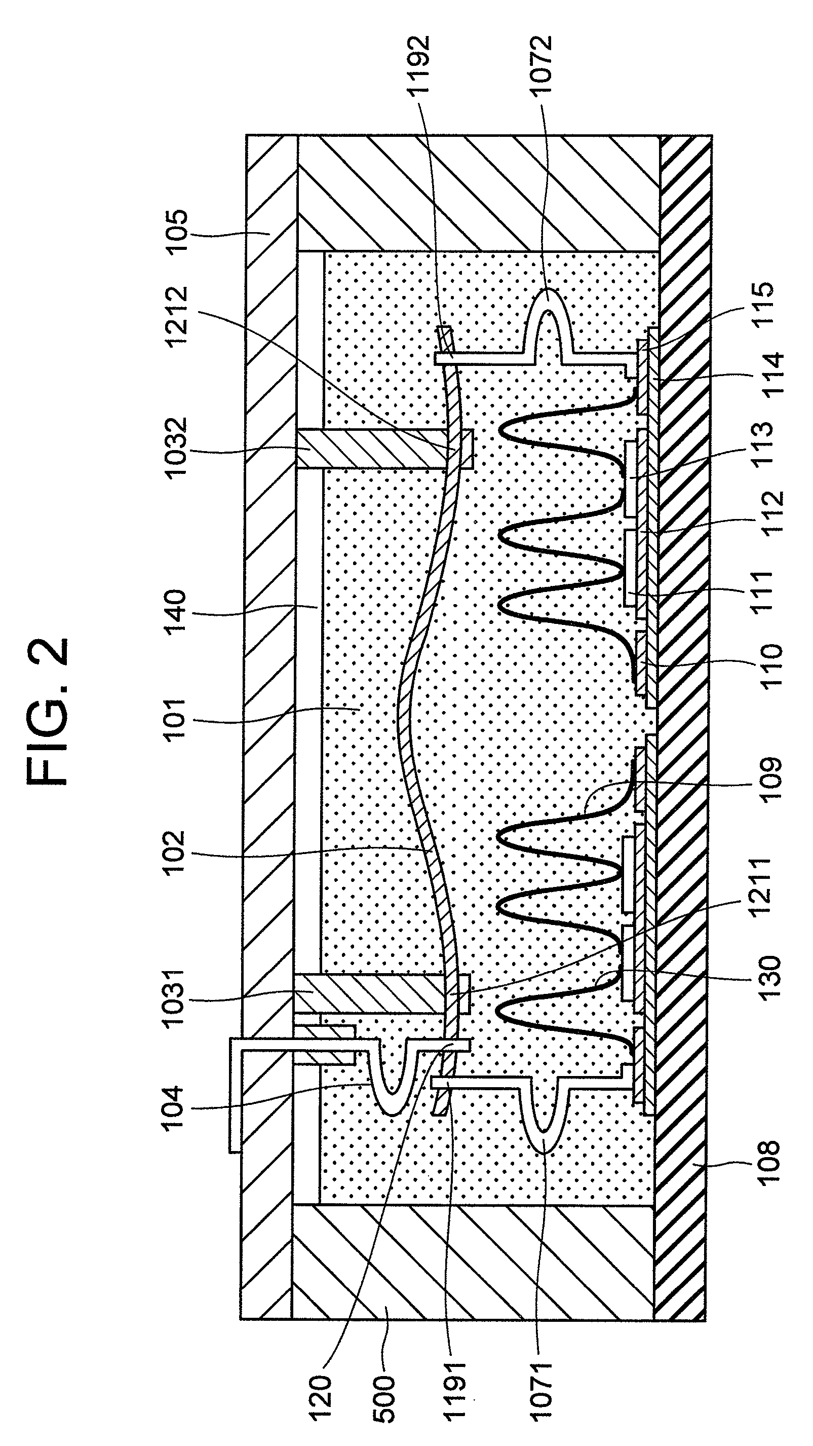
[0036]FIG. 1 is a sectional model view showing a power semiconductor module according to a first embodiment of the present invention. FIG. 2 is a sectional model view showing the power semiconductor module according to the first embodiment of the present invention provided after applying a heat cycle. In FIGS. 1 and 2, an insulating substrate 114 is mounted on a base 108. On the insulating substrate 114 are patterned a conductor 112 for connecting a main terminal, a conductor 115 for connecting a control terminal, and a conductor 110 for connecting the main terminal and the control terminal. On the conductor 112 for the main terminal are mounted an IGBT chip 113 and a diode chip 111. A bonding wire 109 connects the IGBT chip 113 with the diode chip 111 and then leads to the conductor 110 for the control terminal. A wire for connecting the control terminal bonds the IGBT chip 113 with the conductor 115 for connecting the control terminal. Bent control terminal 1071 and 1072 connect t...
second embodiment
[0044]FIG. 6 is a sectional model view showing a power semiconductor module according to a second embodiment of the present invention. The second embodiment is characterized in that bonding wires 1181 and 1182 are used for connecting the conductors 115 for connecting the control terminal with the wiring pattern on the printed board 102 and a bonding wire 117 is used for connecting the wiring pattern on the printed board 102 with the control terminal 116.
[0045]This embodiment is effective in improving the reliability of the power semiconductor module in a power cycle if the printed board 102 is greatly displaced.
[0046]FIG. 7 is a plan view showing a fourth embodiment of the printed board that may be preferably applied to the power semiconductor module according to the present invention. Before describing the fourth embodiment, the relation among a width a of the printed board, a filling depth b of silicon gel located under the printed board 102, and a load Fc applied onto the printed...
third embodiment
[0062]FIG. 15 is a sectional model view showing a power semiconductor module according to the third embodiment of the present invention. The third embodiment is characterized in that part or all of each supporter 1031 or 1032 is made thin as shown by 10311 and 10321 so that the printed board 102 may be moved vertically on the thin supporter served as a guide rail. That is, the supporters 1031 and 1032 movably supports the printed board 102 longitudinally. Hence, the printed board 102 is moved vertically according to expansion or shrinkage of the silicon gel 101. However, the displacement is not conveyed to the supporters 1031 and 1032. This leads to reducing the displacement of the cover plate 104 and thereby preventing the crack of the cover plate 104.
PUM
 Abstract
Description
Claims
Application Information
 - R&D
- Intellectual Property
- Life Sciences
- Materials
- Tech Scout
- Unparalleled Data Quality
- Higher Quality Content
- 60% Fewer Hallucinations
Browse by: Latest US Patents, China's latest patents, Technical Efficacy Thesaurus, Application Domain, Technology Topic, Popular Technical Reports.
© 2025 PatSnap. All rights reserved.Legal|Privacy policy|Modern Slavery Act Transparency Statement|Sitemap|About US| Contact US: help@patsnap.com