Back-Contact Photovoltaic Cells

a photovoltaic cell and back-contact technology, applied in the field of new photovoltaic cells, can solve the problems of increasing the amount of time needed for photovoltaic cells to be manufactured, consuming energy, and using high temperatures

Inactive Publication Date: 2007-12-27
BP CORP NORTH AMERICA INC
View PDF15 Cites 75 Cited by
  • Summary
  • Abstract
  • Description
  • Claims
  • Application Information

AI Technical Summary

Problems solved by technology

However, these are not the only methods used to obtain suitable semiconductor wafers for the manufacture of photovoltaic cells.
Using high temperatures increases the amount of time needed

Method used


Image

  • Back-Contact Photovoltaic Cells
  • Back-Contact Photovoltaic Cells
  • Back-Contact Photovoltaic Cells

Examples


Embodiment Construction

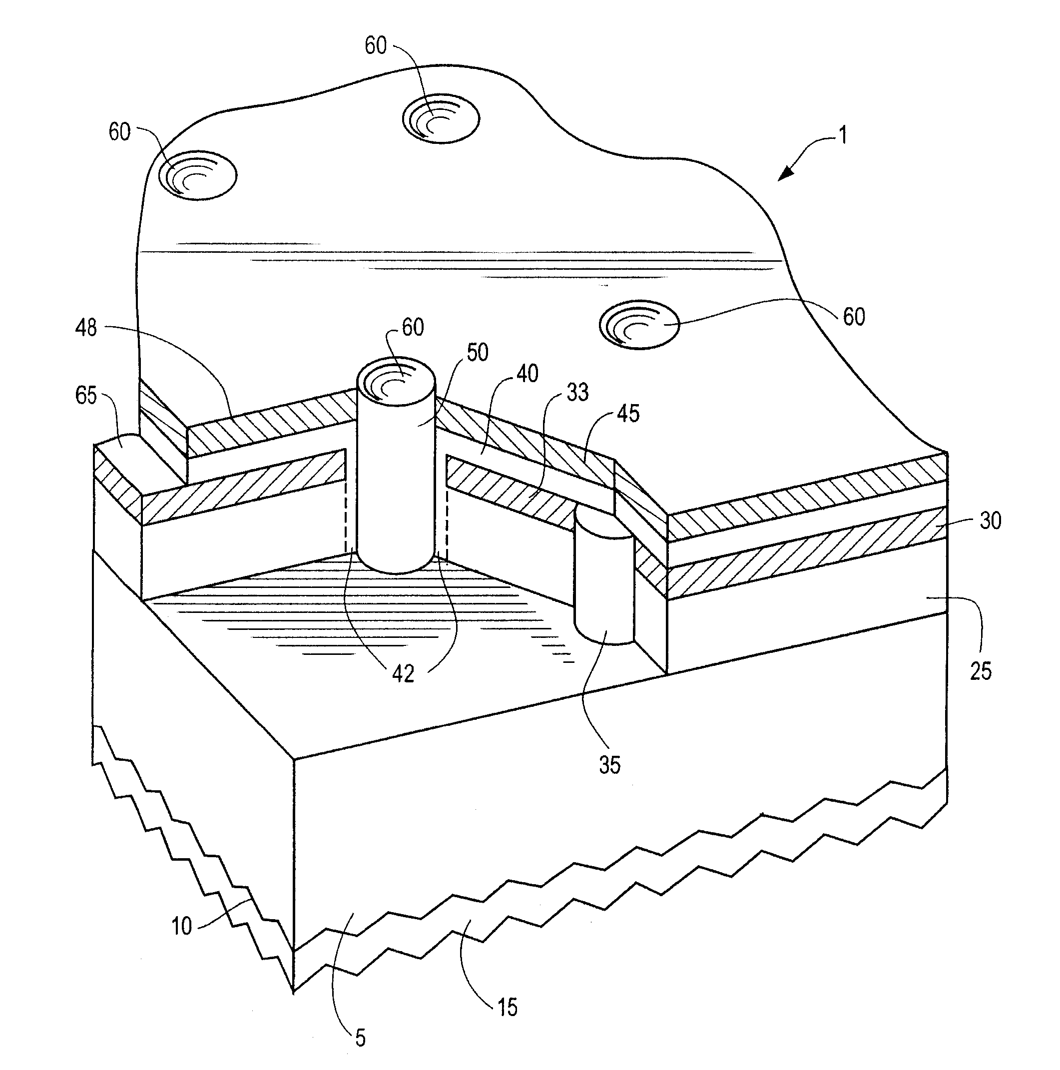
[0017] A semiconductor wafer useful in the process of this invention for preparing photovoltaic cells preferably comprises silicon and is typically in the form of a thin, flat shape. The silicon may comprise one or more additional materials, such as one or more semiconductor materials, for example germanium, if desired. For a p-type wafer, boron is widely used as the p-type dopant, although other p-type dopants, for example, aluminum, gallium or indium, will also suffice. Boron is the preferred p-type dopant. Combinations of such dopants are also suitable. Thus, the dopant for a p-type wafer can comprise, for example, one or more of boron, aluminum, gallium or indium, and preferably it comprises boron. If an n-type silicon wafer is used, the dopants can be, for example, one or more of phosphorus, arsenic, antimony, or bismuth. Suitable wafers are typically obtained by slicing or sawing silicon ingots, such as ingots of monocrystalline silicon, to form monocrystalline wafers, such as...


PUM


Abstract

A photovoltaic cell comprising a wafer comprising a semiconductor material of a first conductivity type, the wafer comprising a first light receiving surface and a second surface opposite the first surface; a first passivation layer positioned over the first surface of the wafer; a first electrical contact comprising point contacts positioned over the second surface of the wafer and having a conductivity type opposite to that of the wafer; and a second electrical contact comprising point contacts and positioned over the second surface of the wafer and separated electrically from the first electrical contact and having a conductivity type the same as that of the wafer.

Description

[0001] This is a continuation-in-part application of U.S. patent application Ser. No. 11 / 565,738, filed on Dec. 1, 2006, which claims the benefit of U.S. Provisional Patent Application 60 / 751,168, filed on Dec. 16, 2005.BACKGROUND OF THE INVENTION [0002] This invention relates to new photovoltaic cells. More particularly, this invention relates to photovoltaic cells that are highly efficient in converting light energy, and particularly solar energy, to electrical energy and where such cells have electrical contacts on the back surface. This invention is also a process for making such cells. [0003] One of the most important features of a photovoltaic cell is its efficiency in converting light energy from the sun into electrical energy. Another important feature is the ability to manufacture such cell in a manner applicable to large-scale manufacturing processes. Thus, the art is continuously striving to not only improve the efficiency of photovoltaic cells in converting light energy ...

Claims


Application Information

Patent Timeline
IPC IPC(8): H01L31/00
CPCH01L31/022433H01L31/02363Y02E10/50H01L31/061
Inventor CARLSON, DAVID E.
Owner BP CORP NORTH AMERICA INC
Why Eureka
Try Eureka