Current Induced Magnetoresistance Device

a current-induced magnetoresistance and magnetic memory technology, applied in the field of current-induced magnetoresistance devices, can solve the problems of increasing the current required, the switching field, and the crosstalk between adjacent lines and cells, and the limitation of increasing the density of the magnetic memory devices, so as to improve the integration

Inactive Publication Date: 2007-12-27
KOREA INST OF SCI & TECH
View PDF7 Cites 21 Cited by
  • Summary
  • Abstract
  • Description
  • Claims
  • Application Information

AI Technical Summary

Benefits of technology

[0010] The CIMS device of the present invention reverses the magnetization direction of the ferromagnetic layers, thereby exhibiting current-induced magnetization switching effect.
[0011] Particularly, since reversing the magnetization of this structure is by a current perpendicular to the plane of layers, it has an advantage of improving the integration

Problems solved by technology

This field-induced magnetization switching method exhibits an inherent disadvantage that the switching field, therefore the required current, is drastically increased with decreasing size of the cells.
Furthermore, crosstalk between the adjoining lines and cells becomes serious when the cell-distance is small.
These put a limitation on increasing the density of the magnetic memory device.
However, there are two critical issues to be solved so that CIMS can be applied in real devices: the switching current density must be lowered and the output signal of the device must be increased.

Method used


Image

  • Current Induced Magnetoresistance Device
  • Current Induced Magnetoresistance Device
  • Current Induced Magnetoresistance Device

Examples


example

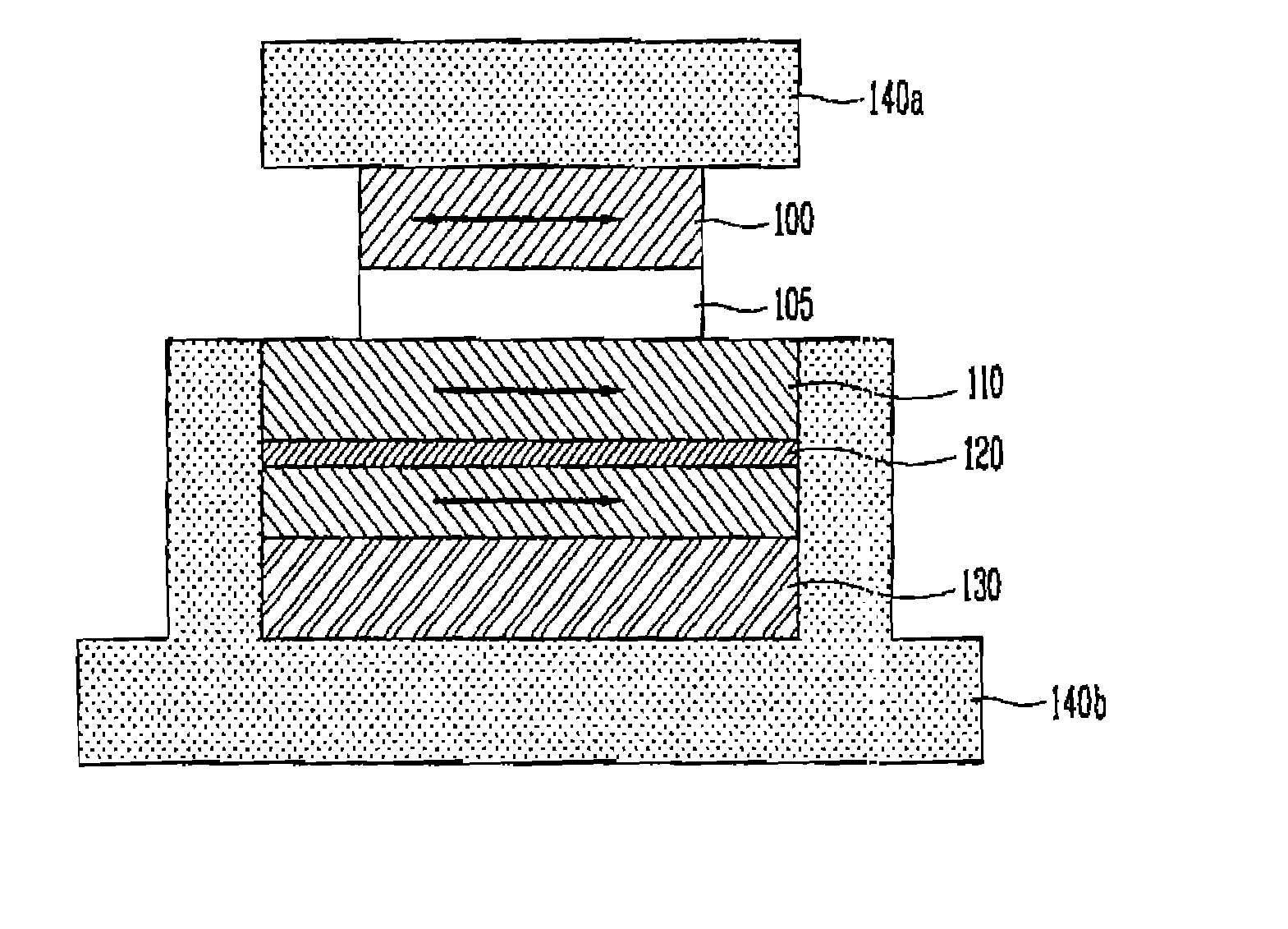
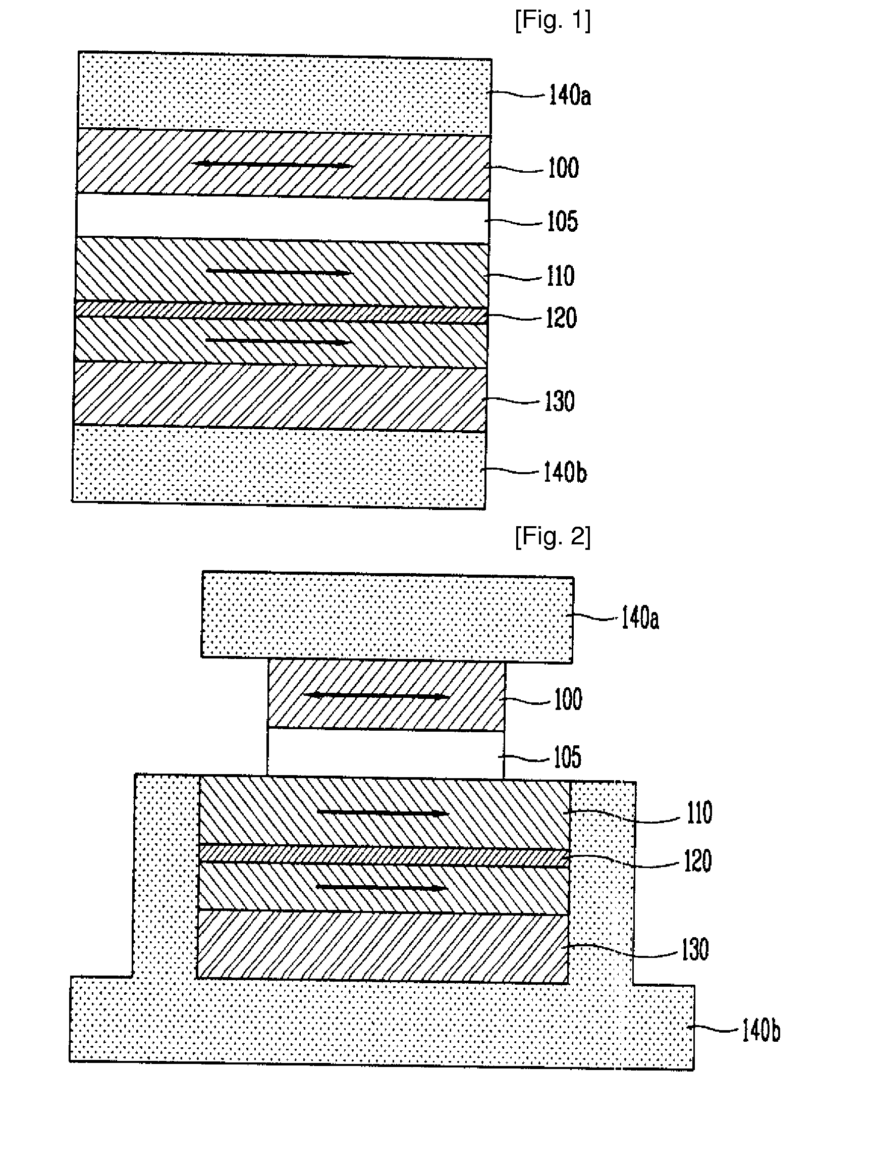
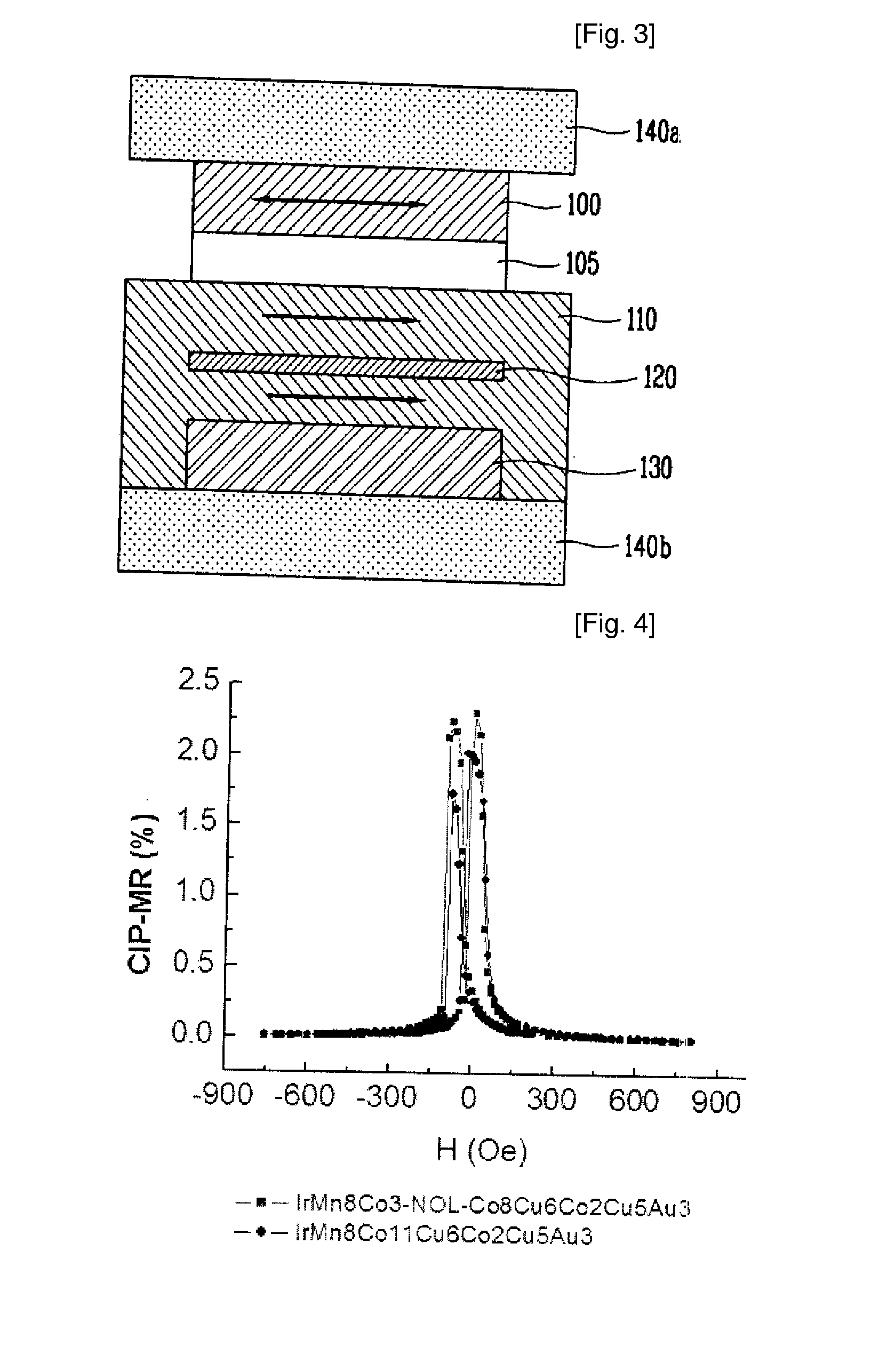
[0028] After preparing the first ferromagnetic layer and the second ferromagnetic layer using cobalt (Co) thins films of 2 nm and 11 nm in thicknesses respectively, the nonmagnetic layer of copper thin film of 6 nm in thickness to be pinned between the ferromagnetic layers was prepared. After forming the first ferromagnetic layer such that it is thinner than the second ferromagnetic layer, an antiferromagnet was formed using IrMn thin film of 8 nm in thickness through exchange coupling at the lower part of the second ferromagnetic layer. In addition, an oxide layer of less than 5 Å was formed when forming the second ferromagnetic layer. The upper part and the lower part of the laminated structure were formed with copper (Cu) electrode of 5 nm respectively, and the lower part of the electrode was formed such that at least a part of the second ferromagnetic layer is in contact with the electrode.

[0029] In order to compare the magnetoresistance device of the present invention, a devic...


PUM


Abstract

The present invention provides for a current induced switching magnetoresistance device comprising a magnetic multilayer composed of a first ferromagnetic layer, a nonferromagnetic layer, and a second ferromagnetic layer, wherein the first ferromagnetic layer has an upper electrode, the second ferromagnetic layer pinned by an antiferromagnet, wherein the antiferromagnet contains a lower electrode at its lower part, and the second ferromagnetic layer is embedded with a nano oxide layer. It is preferable to have at least a part of the lower electrode in contact with the second ferromagnetic layer. The magnetoresistance device of the present invention provides a lower critical current (Ic) for the magnetization reversal and has an increased resistance.

Description

TECHNICAL FIELD [0001] The present invention relates to a current induced magnetoresistance device, more particularly to a newly structured device that, by having an extended exchange biased pinned ferromagnetic thin film with an embedded nano-oxide layer, can be switched at lower current density and simultaneously provides an increasing change in absolute resistance at switching points. BACKGROUND ART [0002] Since a great magnetoresistance (GMR) was discovered in a ferromagnetic thin film, its application has been suggested to various fields. A typical application thereof is a magnetic random access memory (MRAM), which is a solid-state memory that can re-write and read recorded data many times by using magnetization direction of ferromagnets. [0003] A unit cell in an MRAM has a multilayered ferromagnet-laminated structure. The relative alignment (being parallel or antiparallel) of the magnetization of the multilayers that consists the memory cell corresponds to “0” or “1” in binar...

Claims


Application Information

Patent Timeline
Patent Type & Authority Applications(United States)
IPC IPC(8): H01L43/08G01R33/09G11C11/16
CPCB82Y25/00H01F10/3259H01L43/08G11C11/15H10N50/10
Inventor SHIN, KYUNG-HOHOANY YEN, NGUYEN THIYI, HYUN-JUNG
Owner KOREA INST OF SCI & TECH
Why Eureka
Try Eureka