Baking method of quartz products, computer program and storage medium

a technology of quartz products and computer programs, applied in the field of baking methods of quartz products, computer programs and storage media, can solve the problems of increasing the possibility of copper contamination, increasing the depth of copper contamination, and leaving a trace amount of copper in the surface portion of quartz products, so as to suppress the degradation of yield and improve the depth of copper concentration

Active Publication Date: 2007-12-27
TOKYO ELECTRON LTD
View PDF3 Cites 10 Cited by
  • Summary
  • Abstract
  • Description
  • Claims
  • Application Information

AI Technical Summary

Benefits of technology

[0010]The present invention was made under such circumstances as described above, and therefore it is an object of this invention to provide a baking method of a quartz product used as a part of a heat treatment apparatus which serves as a semiconductor manufacturing apparatus, wherein the quartz product can suppress copper contamination of semiconductor substrates.
[0011]The present invention is a baking method of a quartz product, which is placed in a reaction vessel for containing semiconductor substrates and providing a heat treatment thereto, and at least a portion of which is located in a heating atmosphere in the reaction vessel, the baking method comprising the steps of: placing the quartz product before subjected to the heat treatment, in the reaction vessel; and supplying baking gases, including a hydrogen chloride gas and a gas for enhancing reactivity of the hydrogen chloride gas, into the reaction vessel, while heating the reaction vessel, for removing copper as a contaminant incorporated during the manufacturing process of the quartz product, whereby the copper concentration in the region from the surface to the 30 μm depth of the quartz product can be controlled below 20 ppb.
[0014]The present invention is a baking method of a quartz product, which is placed in a reaction vessel for containing semiconductor substrates and providing a heat treatment thereto, and at least a portion of which is located in a heating atmosphere in the reaction vessel, the baking method comprising the steps of: placing the quartz product before subjected to the heat treatment, in the reaction vessel; and supplying baking gases, including a hydrogen chloride gas and a gas for enhancing reactivity of the hydrogen chloride gas, into the reaction vessel, while heating the reaction vessel, for removing copper as a contaminant incorporated during the manufacturing process of the quartz product, whereby the copper concentration in the region from the surface to the 10 μm depth of the quartz product can be controlled below 10 ppb.
[0034]According to the present invention, it can be found that, in the quartz product which is a part of the heat treatment apparatus, the copper contamination, which is generated on the manufacturing stage, is not only present at the surface of the quartz but also penetrates into the interior, and the profile of the copper concentration in the depth direction can be improved by baking the quartz product. Since the quartz product which exhibits a significantly low degree of copper contamination can be provided due to the improvement of the copper concentration profile, the copper contamination to semiconductor substrates to be heated by the heat treatment apparatus which is composed of such a quartz product can be surely reduced, thereby suppressing degradation of the yield.

Problems solved by technology

While such quartz products are machined through various steps starting from a quartz ingot, metallic contamination due to copper or the similar metal tends to occur because of contact with machining tools or effect from the working atmosphere.
In particular, for the wafer boat, supporting portions for supporting wafers are composed of grooves or nails and require fine machining works for their formation, as such increasing the possibility of copper contamination.
However, the copper ions eluted into the hydrofluoric acid may tend to be coupled again to uncoupled sites of silicon atoms, resulting in leaving a trace amount of copper in the surface portion of the quartz products.
In this case, if the surface portion of each quartz product is contaminated with even a trace amount of copper, when the user starts the operation of the apparatus to carry out a heat treatment of wafers, the copper is heated up so as to make the molecular movement vigorous, as such a part of the copper is scattered into the heating atmosphere, then attaches to wafers and causes contamination of the wafers.
Accordingly, even though the wafer is contaminated by a trace amount of copper, electric characteristics of semiconductor devices may be badly affected, thus lowering the yield.
Therefore, the assessment for the copper a contamination of quartz products based only on the number of copper atoms in the surface portion of the quartz products can not successfully meet the prevention of wafer contamination.Patent Document 1: TOKUKAI No. 2002-313787 (claim 1, Paragraphs to )

Method used


Image

  • Baking method of quartz products, computer program and storage medium
  • Baking method of quartz products, computer program and storage medium
  • Baking method of quartz products, computer program and storage medium

Examples


examples

[0065]Next, results obtained by a specific baking method for obtaining the quartz products of the present invention will be described.

A. Preparation of an Object to be Tested and a Testing Method

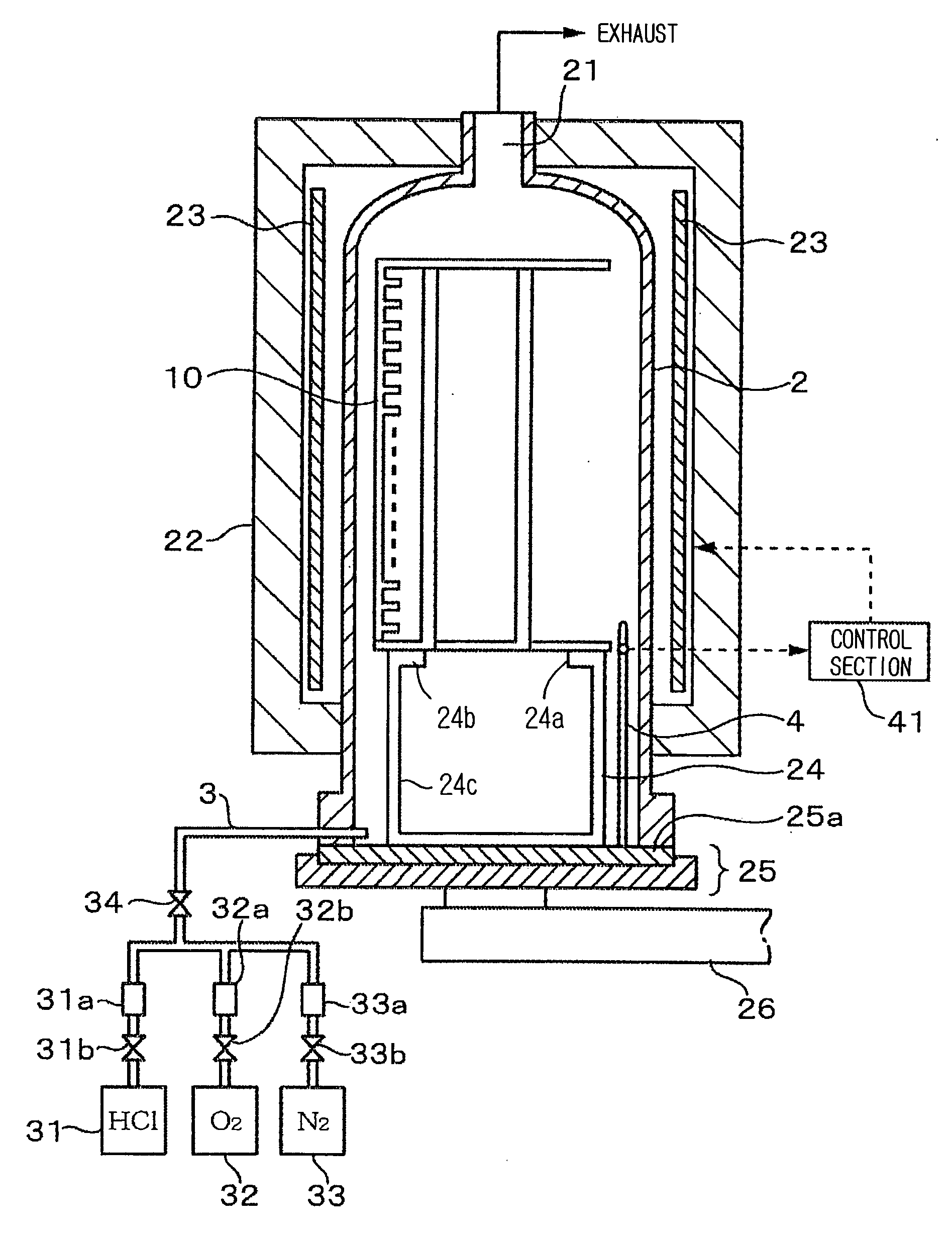
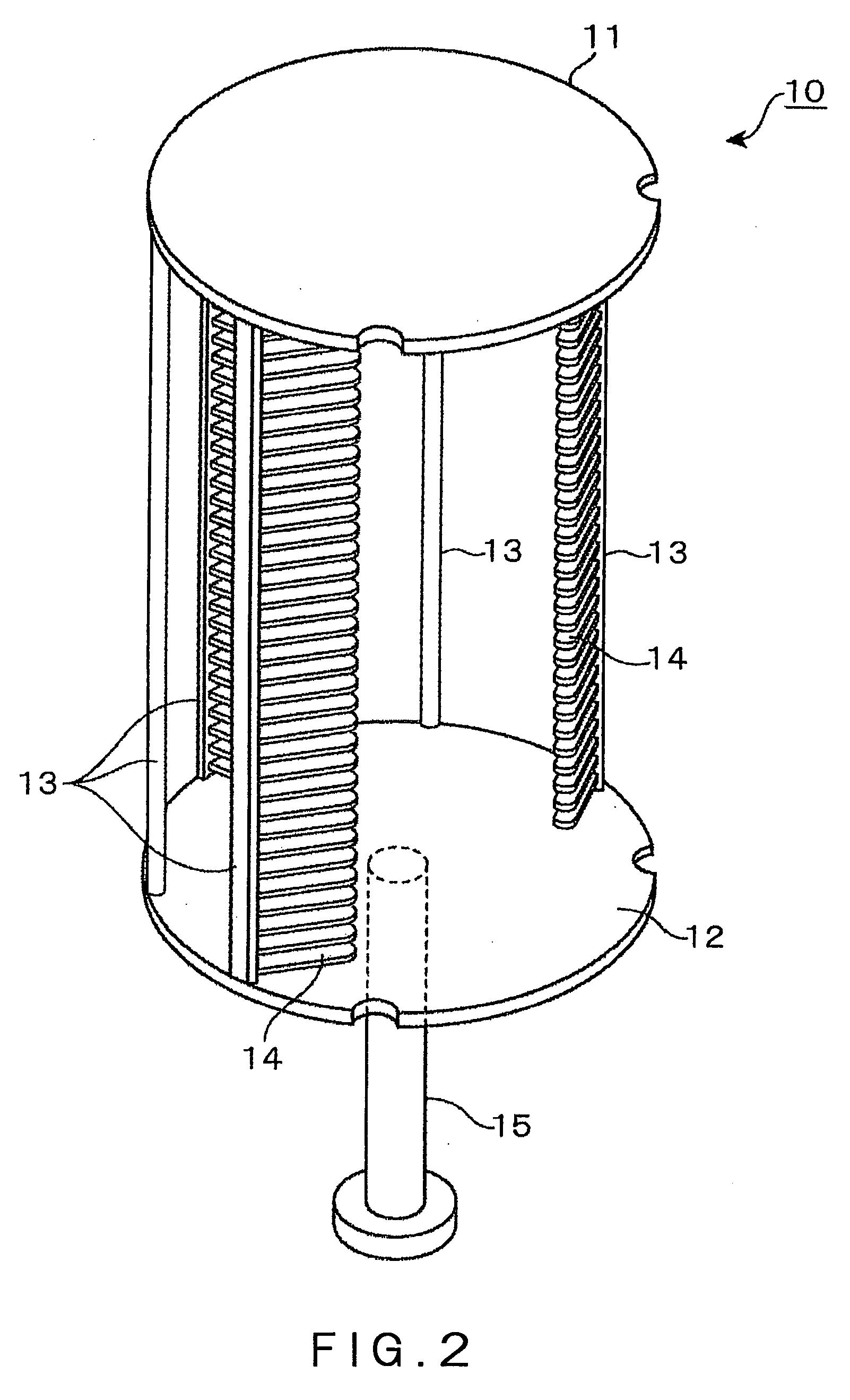
[0066]An object to be tested was prepared by cutting a nail portion of the wafer boat by using a diamond cutter. In this case, the wafer boat was shown in FIG. 2 and delivered from a quartz product maker. Using hydrofluoric acid, the surface of the object was etched up to the 10 μm depth. Thereafter, the object to be tested was placed on a silicon-bear wafer mounted on a quartz jig, and the jig was then carried into the baking furnace shown in FIG. 1. In the baking furnace, the baking process according to the method of the present invention had been carried out in advance, and the jig had been previously subjected to the baking process according to the method of present invention in the baking furnace. Therefore, there was no risk that the object to be tested was contaminated with copper due...


PUM

PropertyMeasurementUnit
temperatureaaaaaaaaaa

Abstract

The present invention relates to control of copper contamination to semiconductor substrates upon operation of a heat treatment apparatus which is a semiconductor manufacturing apparatus and which is constructed with quartz products having been contaminated with copper when machined. The quartz product is placed in a heating atmosphere on the stage where it is not still used for a heat treatment for semiconductor substrates. Baking gases including a hydrogen chloride gas and a gas for enhancing activity of the hydrogen chloride gas, for example, an oxygen gas, are then supplied to the quartz product. Consequently, the copper concentration in the region from the surface to the 30 μm depth of the quartz product can be controlled below 20 ppb, preferably below 3 ppb. The baking process may be carried out before or after assembling the quartz product into the heat treatment apparatus.

Description

BACKGROUND OF THE INVENTION[0001]1. Field of the Invention[0002]The present invention relates to a technique for removing metals contained in a quartz product by baking the quartz product which is a component of a heat treatment apparatus for heating semiconductor substrates.[0003]2. Background Art[0004]As one example of the heat treatment apparatus used in a semiconductor manufacturing process, there is known a vertical-type heat treatment apparatus which is a batch-type heat treatment apparatus. This vertical-type heat treatment apparatus comprises a heating furnace including a vertical-type reaction vessel which opens downwardly and a heater provided to surround the outside of the reaction vessel. Multiple sheets of semiconductor wafers (hereinafter referred to as wafers) are held in a shelf-like state by a wafer holding tool called wafer boat and carried into the reaction vessel from below, so as to perform a film forming process or the like, by oxidation, diffusion process or C...

Claims


Application Information

Patent Timeline
Patent Type & Authority Applications(United States)
IPC IPC(8): H01L21/02
CPCH01L21/67306Y10S438/905Y10S438/935C23C16/44H01L21/22H01L21/31H01L21/324
Inventor ANBAI, KATSUHIKOOIKAWA, MASAYUKISHIBATA, TETSUYATANI, YUICHI
Owner TOKYO ELECTRON LTD
Why Eureka
Try Eureka