Photovoltaic device which includes all-back-contact configuration; and related processes

Inactive Publication Date: 2008-01-03
GENERAL ELECTRIC CO
View PDF17 Cites 77 Cited by
  • Summary
  • Abstract
  • Description
  • Claims
  • Application Information

AI Technical Summary

Problems solved by technology

Moreover, polycrystalline semiconductor materials may contain randomly-oriented grains, with grain boundaries which induce a large number of bulk and surface defect sites.
The presence of various defects of this type can be the source of deleterious effects in the photovoltaic device.
Thus, they become lost as current carriers.
This new interface is yet another site for impurities and spurious contaminants to become trapped and to accumulate, and possibly cause additional recombination of the charge carriers.
As an example, interruptions between the deposition steps during fabrication of a multilayer structure can provide unwelcome opportunities for the entry of the contaminants.
Moreover, abrupt band bending at the interface, due to a change in conductivity, and/or variations in band gap, can lead to a high density of interface states, which is another

Method used


Image

  • Photovoltaic device which includes all-back-contact configuration; and related processes
  • Photovoltaic device which includes all-back-contact configuration; and related processes
  • Photovoltaic device which includes all-back-contact configuration; and related processes

Examples


examples

[0069]A general example is provided below. It should be viewed as merely illustrative, and should not be construed to be any sort of limitation on the scope of the claimed invention.

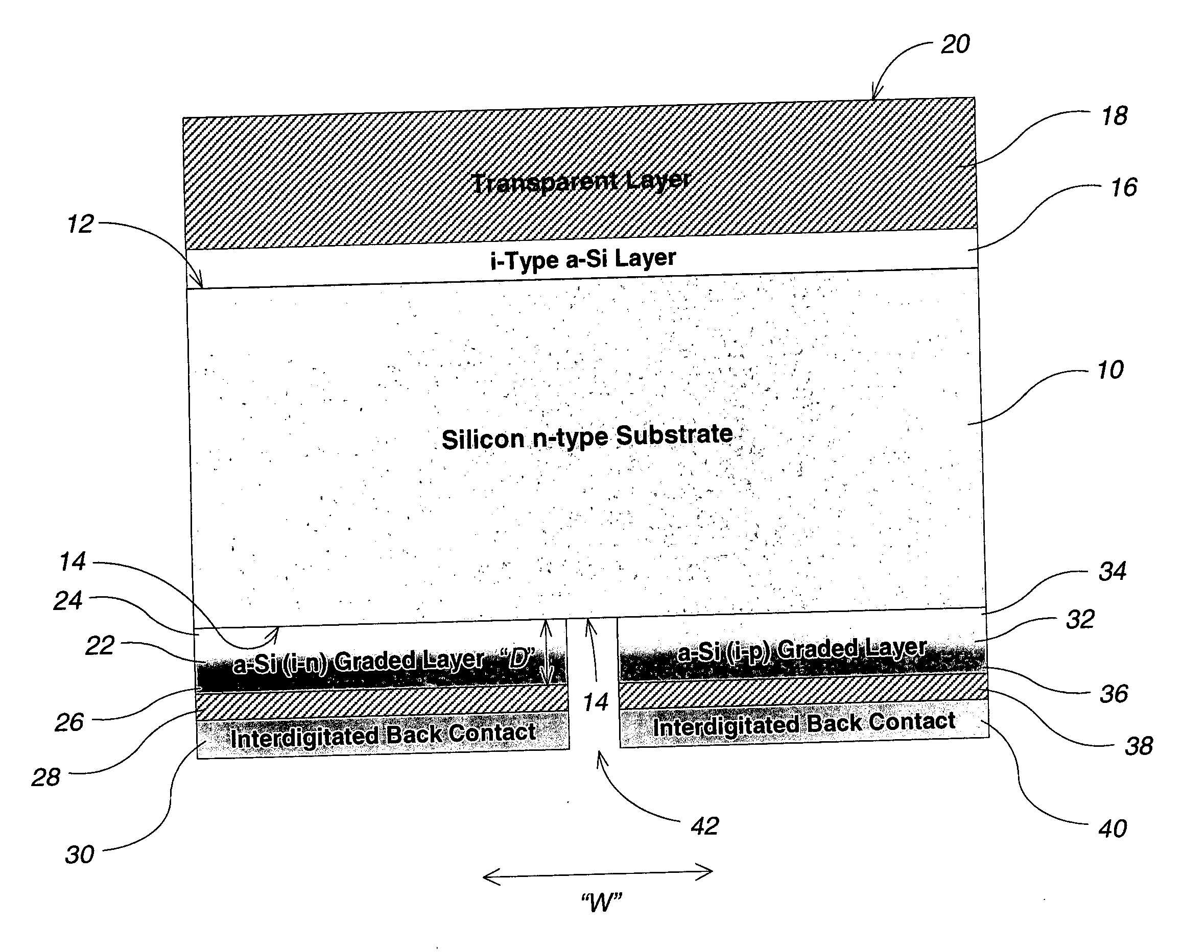
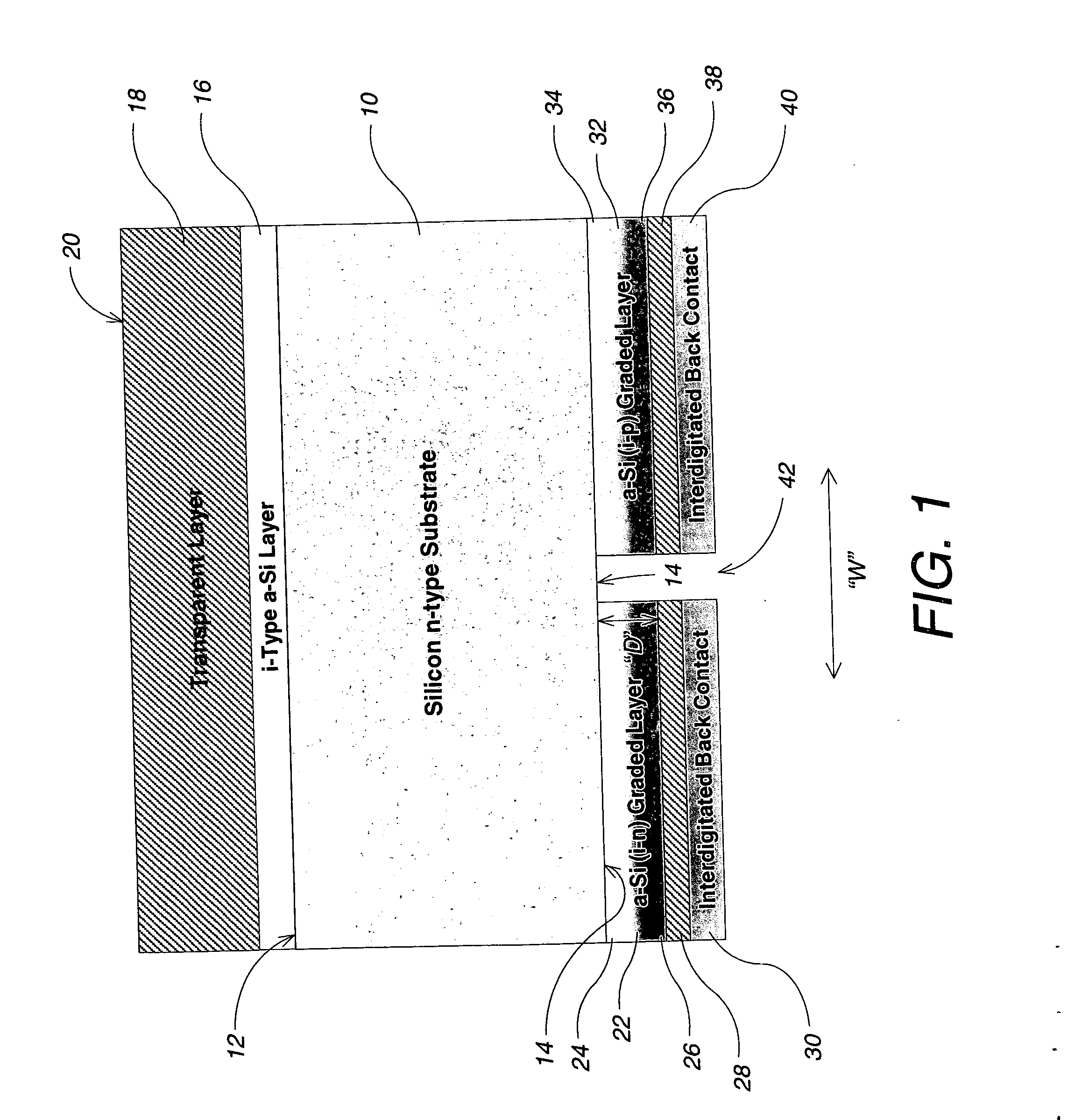
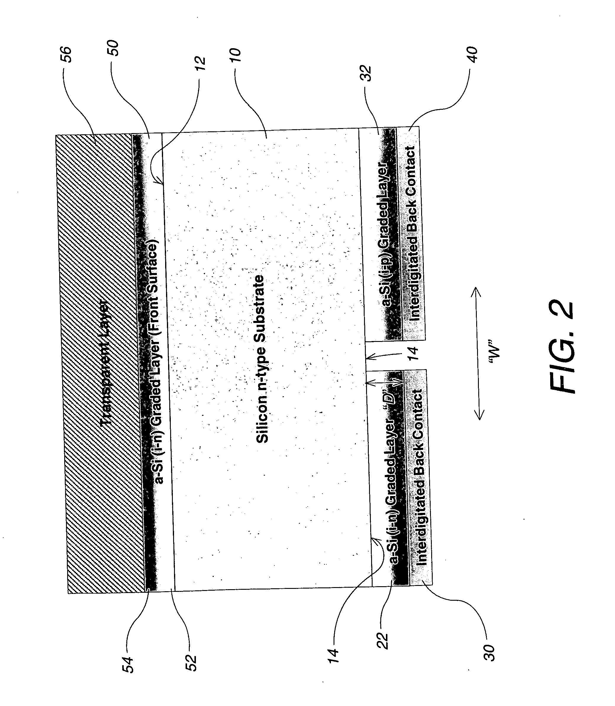
[0070]The fabrication of photovoltaic devices according to some embodiments of the present invention can be undertaken as follows: Monocrystalline or polycrystalline semiconductor substrates (or silicon wafers) of one conductivity type can first be etched by conventional techniques. For example, a texturing solution containing selected proportions of ultra-pure deionized water, potassium hydroxide (KOH, 45% concentration), and isopropyl alcohol can first be prepared in a quartz vessel. The temperature of the texturing solution is usually maintained at about 65° C.-80° C. The substrate can then be immersed in the agitated solution for a period of time determined to be suitable to achieve the desired degree of etching (typically about 5-60 minutes). Following the texturing step, the substrate is removed an...


PUM


Abstract

A semiconductor structure is described, which includes a semiconductor substrate of one conductivity type, having a front surface and a back surface. A first amorphous semiconductor layer is applied on the front surface; and second and third amorphous semiconductor layers are disposed on portions of the back surface of the substrate. The second and third layers are each compositionally graded through their depth, from substantially intrinsic at the interface with the substrate, to substantially conductive at their opposite surfaces. In some instances, the first semiconductor layer is also compositionally graded, while in other instances, it is intrinsic in character. The semiconductor structures can function as solar cells; and modules which include a number of such cells represent another embodiment of the invention. Methods for making a photovoltaic device are also described.

Description

BACKGROUND OF THE INVENTION[0001]This invention relates generally to high efficiency solar cells. More specifically, the invention relates to solar cells based on semiconductor devices which include a heterojunction.[0002]There is no doubt that solar energy offers the potential for providing virtually unlimited energy for use by man, if the solar energy can be made available in a useful form. Perhaps the greatest effort so far as been in using the sun's energy to obtain electricity, which can then be utilized through any existing electrical network—on the household, community, or industrial level. A primary approach to generating this electricity from solar radiation has involved direct generation by way of photovoltaic converters. These types of devices rely on the presence of a heterojunction, and are well-known in the art. (As used in this context, a heterojunction is a semiconductor junction which is composed of layers of dissimilar semiconductor material. These materials usuall...

Claims


Application Information

Patent Timeline
IPC IPC(8): H01L31/00H02N6/00H01L31/068
CPCH01L31/0747H01L31/20H01L31/065H01L31/02167H01L31/02363Y02E10/50Y02E10/547H01L31/04H01L31/06
Inventor JOHNSON, JAMES NEILMANIVANNAN, VENKATESAN
Owner GENERAL ELECTRIC CO
Why Eureka
Try Eureka