High efficiency thermoelectric materials based on metal/semiconductor nanocomposites

a technology of thermoelectric materials and nano-composites, which is applied in the direction of thermoelectric device junction materials, conductive materials, conductors, etc., can solve the problems of difficult integration with electronic devices fabricated on silicon, and achieve the effects of increasing the electrical conductivity of materials, large seebeck coefficients, and high electrical conductivity

Active Publication Date: 2008-01-03
RGT UNIV OF CALIFORNIA
View PDF1 Cites 12 Cited by
  • Summary
  • Abstract
  • Description
  • Claims
  • Application Information

AI Technical Summary

Benefits of technology

[0012] Also, some semiconductors, such as the InGaAlAs used in the present invention have multiple valleys in their conduction band which can become accessible with large electron concentrations. In this case, the L-valley states would drastically increase the electrical conductivity of the material. At the same time, the electrostatic Schottky barriers around the particle serve as energy-dependent electron scatterers. This results in a higher electrical conductivity from high energy carriers than low energy carriers and therefore a large Seebeck coefficient.
[0013] The presence of L-valley conduction can also increase the high-energy-carrier conduction, further increasing the Seebeck coefficient. A similar and related technique would be to use a wider-bandgap semiconductor to form conduction band barriers in a small bandgap semiconductor with metal nanoparticles. In this case, the intrinsic carriers would be the primary source of holes (p-type charge carriers) at high temperatures. An equal number of electrons are produced, but their motion is blocked by the barriers. As a result, a high electrical conductivity results (in this case, with holes as the charge carriers), but the Seebeck coefficient remains high because the Fermi level tends towards midgap due to the presence of electrons in the conduction band.

Problems solved by technology

These devices are difficult to integrate with electronic devices fabricated on silicon.

Method used


Image

  • High efficiency thermoelectric materials based on metal/semiconductor nanocomposites
  • High efficiency thermoelectric materials based on metal/semiconductor nanocomposites
  • High efficiency thermoelectric materials based on metal/semiconductor nanocomposites

Examples


Embodiment Construction

[0027] In the following description, reference is made to the accompanying drawings which form a part hereof, and which is shown, by way of illustration, several embodiments of the present invention. It is understood that other embodiments may be utilized and structural changes may be made without departing from the scope of the present invention.

Overview

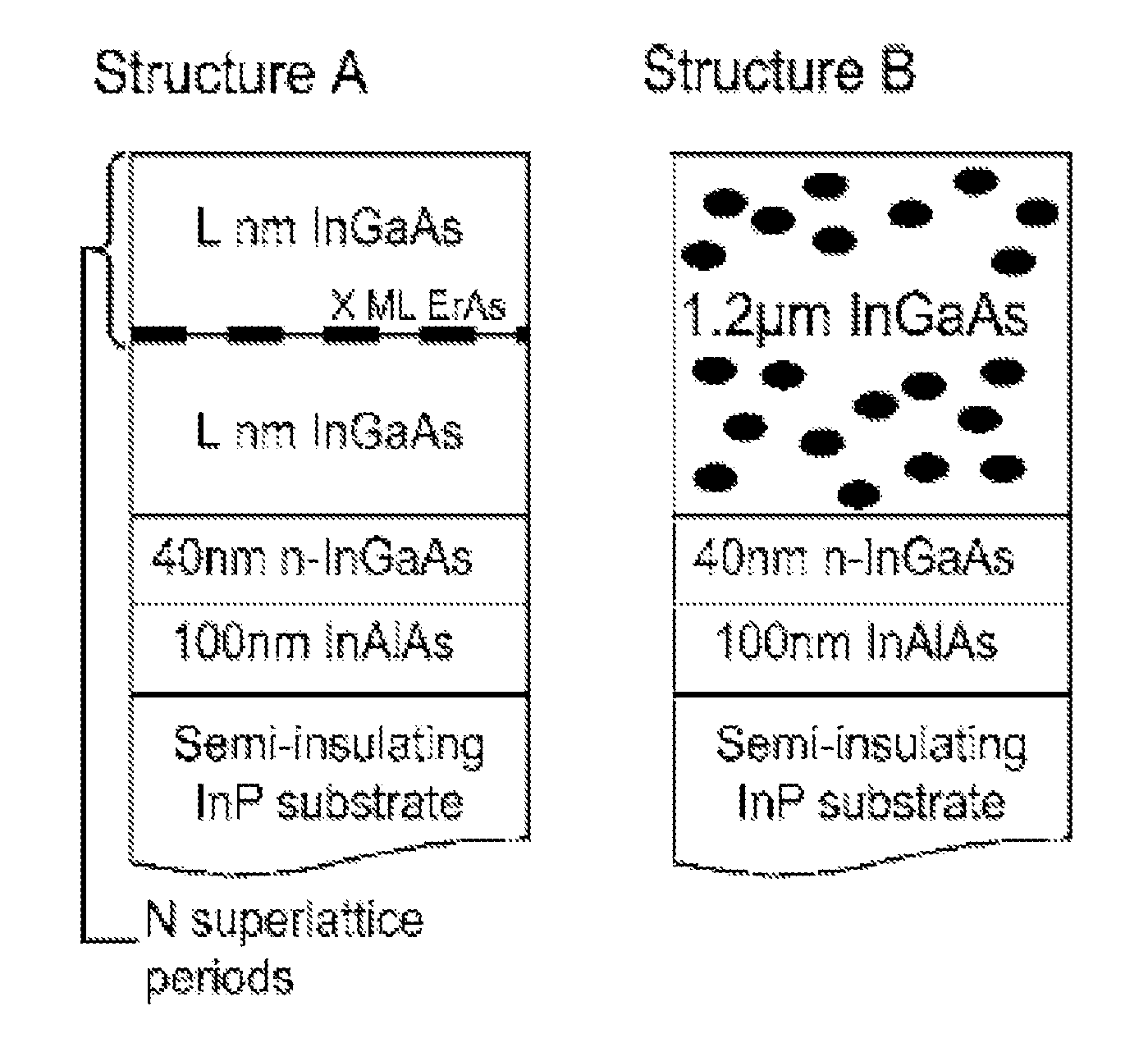
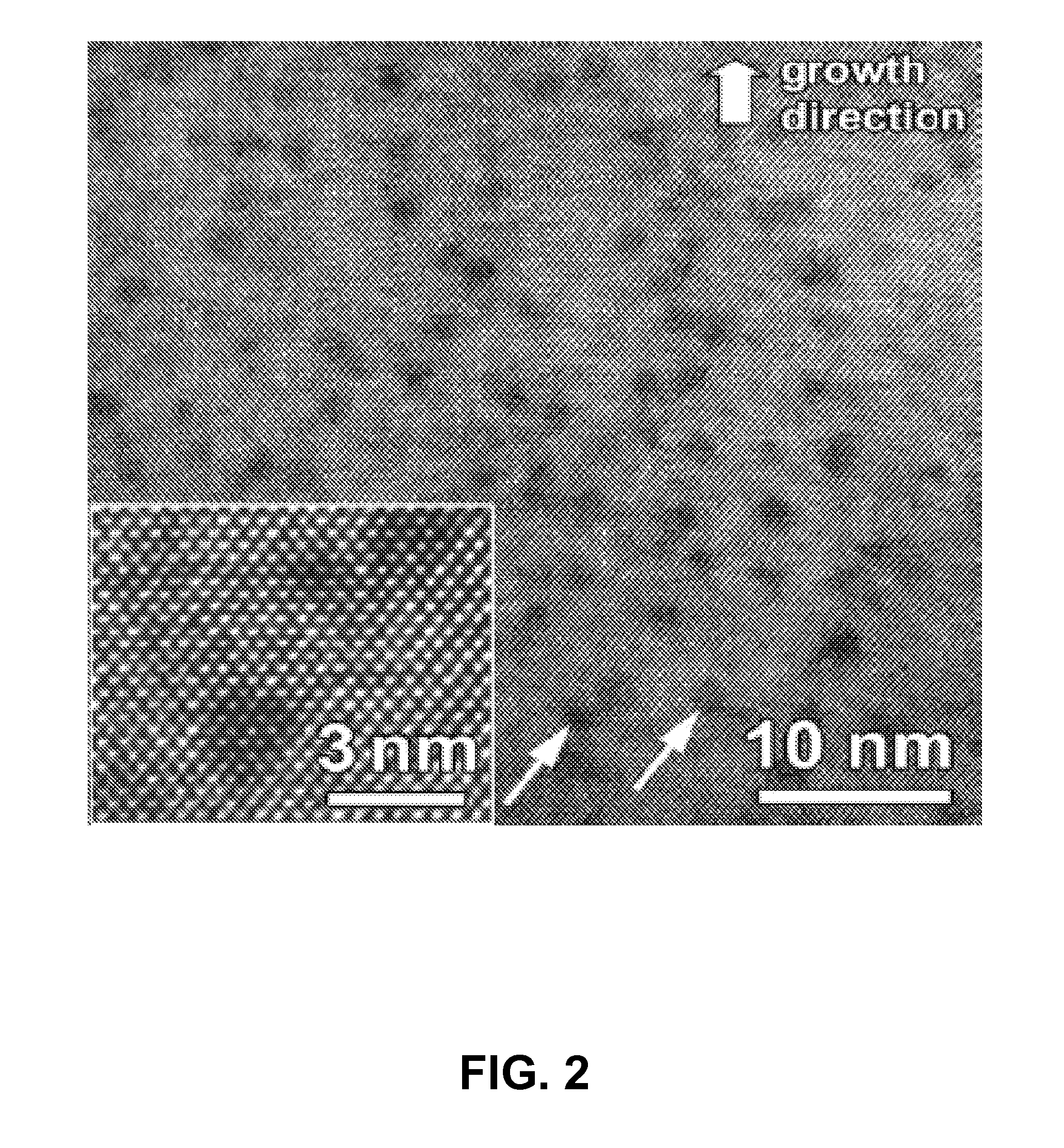
[0028] The big advantage of nanoparticle materials over existing materials for energy conversion devices is the potential for a much higher power factor and ZT, which would lead to a drastic increase in efficiency. The inclusion of nanoparticles provides a novel way of increasing conductivity with temperature through deep-level doping and also increase Seebeck coefficient through energy-dependent scattering. Additionally, the inclusion of ErAs decreases thermal conductivity, increasing ZT further.

[0029] The present invention further provides advantages in thermoelectric power generation for waste heat recovery, e.g., automobiles...


PUM

PropertyMeasurementUnit
temperaturesaaaaaaaaaa
total thicknessaaaaaaaaaa

Abstract

Composite epitaxial materials that comprise semimetallic ErAs nanoparticles or nanoislands epitaxially embedded in a semiconducting In0.53Ga0.47As matrix both as superlattices and randomly distributed throughout the matrix are disclosed. The presence of these particles increases the free electron concentration in the material while providing scattering centers for phonons. Electron concentration, mobility, and Seebeck coefficient of these materials are discussed and their potential for use in thermoelectric power generators is postulated. These composite materials in accordance with the present invention have high electrical conductivity, low thermal conductivity, and a high Seebeck coefficient. The ErAs nanoislands provides additional scattering mechanism for the mid to long wavelength phonon—the combination reduces the thermal conductivity below the alloy limit.

Description

CROSS-REFERENCE TO RELATED APPLICATIONS [0001] This application claims the benefit under 35 U.S.C. Section 119(e) of co-pending and commonly-assigned U.S. provisional patent application, Ser. No. 60 / 815,159, titled Jun. 19, 2006, entitled “HIGH EFFICIENCY THERMOELECTRIC MATERIALS BASED ON METAL / SEMICONDUCTOR NANOCOMPOSITES,” by Joshua M. O. Zide et al., which application is incorporated by reference herein.STATEMENT REGARDING FEDERALLY SPONSORED RESEARCH AND DEVELOPMENT [0002] This invention was made with Government support under Grant No. 442530-23110-3, Grant No. 442530-23104, and Grant No. N00014-03-1-0790, awarded by the ONR. The Government has certain rights in this invention.BACKGROUND OF THE INVENTION [0003] 1. Field of the Invention [0004] The present invention relates generally to semiconductor devices, and, more specifically, to high efficiency thermoelectric materials based on Metal / Semiconductor nanocomposites. [0005] 2. Description of the Related Art [0006] Semiconducto...

Claims


Application Information

Patent Timeline
Patent Type & Authority Applications(United States)
IPC IPC(8): H01B1/02
CPCH01L21/02392H01L21/02463H01L21/02502H01L35/26H01L21/02601H01L35/18H01L21/02546H10N10/857H10N10/853
Inventor ZIDE, JOSHUA M. O.GOSSARD, ARTHUR C.SHAKOURI, ALIBOWERS, JOHN E.
Owner RGT UNIV OF CALIFORNIA
Why Eureka
Try Eureka