Correction method and correction system for design data or mask data, validation method and validation system for design data or mask data, yield estimation method for semiconductor integrated circuit, method for imporving design rule, mask production method, and semiconductor integrated circuit production method

Inactive Publication Date: 2008-01-03
SHARP KK
View PDF23 Cites 68 Cited by
  • Summary
  • Abstract
  • Description
  • Claims
  • Application Information

AI Technical Summary

Benefits of technology

[0051]The present invention is made in view of the foregoing conventional problems, and an object is to provide correction method and correction system for mask pattern data, validation method and validation system for mask pattern data for ensuring the process spec (including the process margin) after a PPC process. With the assurance of the process spec, the present invention prevents wastes in cost and development period due to

Problems solved by technology

In the design data or the mask data corrected by the conventional imperfect PPC, there has been a problem of discordance between the pattern size measured aft

Method used


Image

  • Correction method and correction system for design data or mask data, validation method and validation system for design data or mask data, yield estimation method for semiconductor integrated circuit, method for imporving design rule, mask production method, and semiconductor integrated circuit production method
  • Correction method and correction system for design data or mask data, validation method and validation system for design data or mask data, yield estimation method for semiconductor integrated circuit, method for imporving design rule, mask production method, and semiconductor integrated circuit production method
  • Correction method and correction system for design data or mask data, validation method and validation system for design data or mask data, yield estimation method for semiconductor integrated circuit, method for imporving design rule, mask production method, and semiconductor integrated circuit production method

Examples


Embodiment Construction

Explanation of the Present Invention

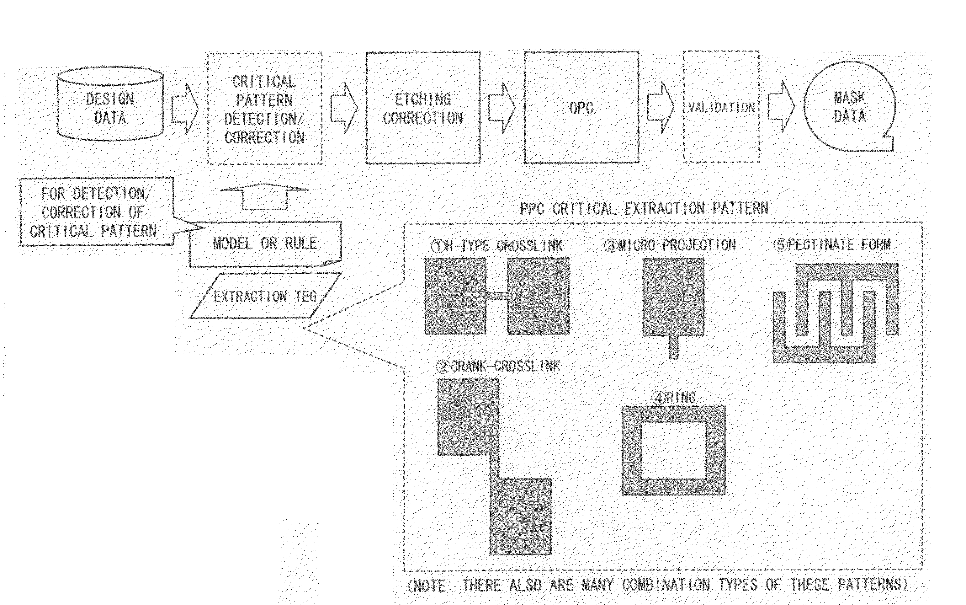
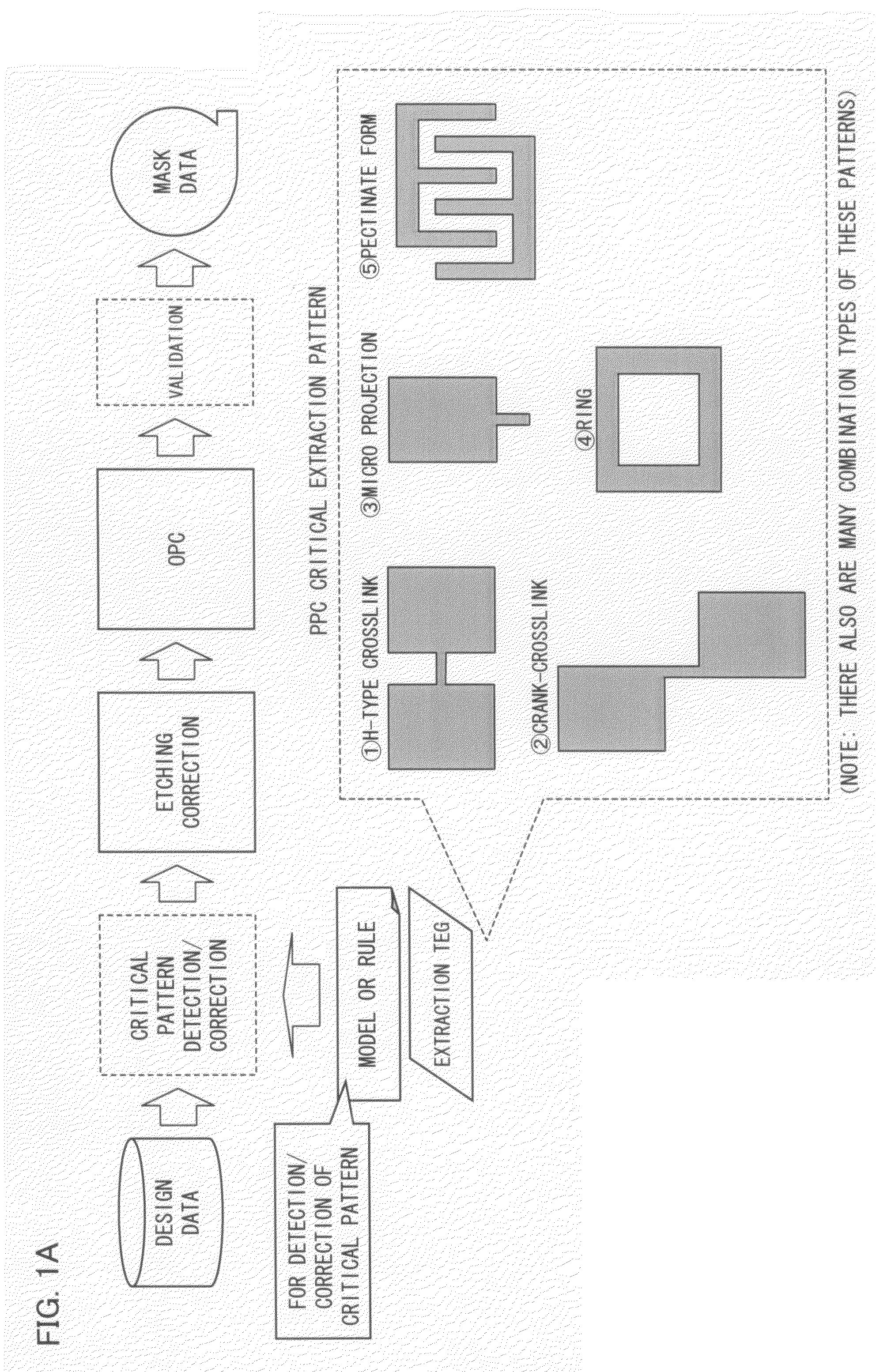
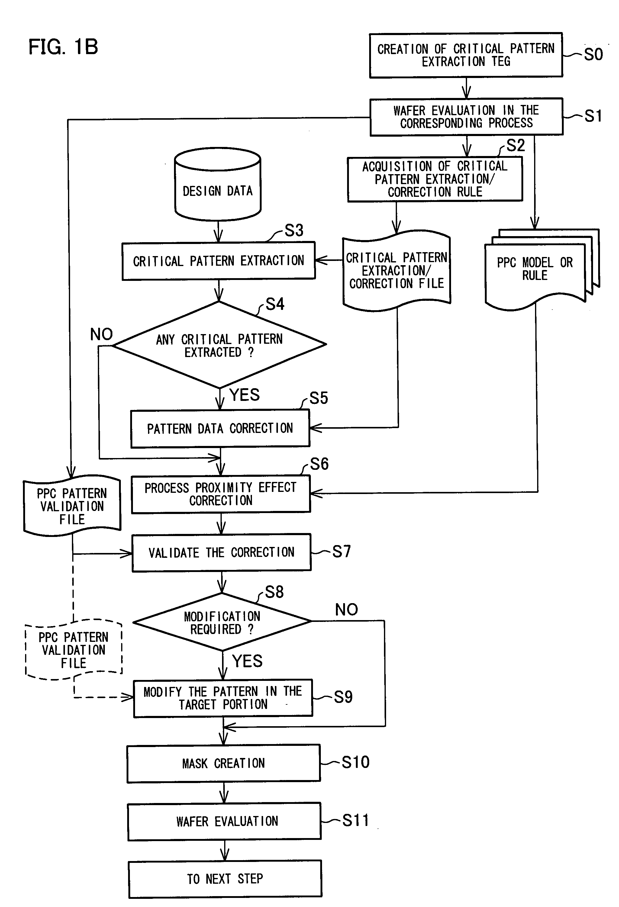
[0091]FIG. 1A shows an example of PPC process flow according to the present invention. FIG. 1B shows the details. In this example of PPC process flow of FIG. 1A, a PPC critical pattern is extracted by an extraction TEG (PPC critical extraction pattern) so as to correct the layout. The layout correction is reflected to the design rule if possible. With this the layout does not need to be corrected in the designing thereafter. In this PPC process flow, it is not necessary to reproduce the design data according to a validation result. A short-circuit prevention pattern and a line-breakage prevention pattern are required as a PPC critical extraction pattern.

[0092]Note that, in the present specification, unless otherwise specified, “the process proximity effect correction” designates not only correction only with respect to shift in the etching process after the exposure (etching proximity effect correction), but also such as correction for correcting ...


PUM


Abstract

The subject invention provides a correction method for design data or mask data comprising the steps of:
    • (i) carrying out PPC of design data or mask data;
    • (ii) exposing and developing a resist with an evaluation mask including a critical pattern which becomes critical in a process, etching a circuit material using the resist having been developed, and measuring pattern sizes of the developed resist and the etched circuit material; (iii) extracting parameter numerical condition for preventing the design data or the mask data from being critical after OPC or PPC, as a rule or as a model based on the pattern sizes of the resist and the circuit material; (iv) extracting a critical pattern with a parameter not satisfying the foregoing rule or the model from the design data or the mask data; and (v) correcting the critical pattern.
With this method, the present invention provides such as a validation/correction method for design data or mask data by which a pattern which becomes critical in a process is extracted in advance so that the pattern can be corrected. Consequently, the process spec is achieved in a short period of time after OPC or process proximity effect correction (PPC).

Description

[0001]This Nonprovisional application claims priority under 35 U.S.C. § 119(a) on Patent Application No. 2006 / 179489 filed in Japan on Jun. 29, 2006, and No. 2007 / 161906 (filed in Japan on Jun. 19, 2007, the entire contents of which are hereby incorporated by reference.FIELD OF THE INVENTION[0002]The present invention relates to a validation method for mask pattern data or design (layout data) used for lithography processes for manufacturing circuit patterns of ICs (integrated circuit), LSIs (large-scale integrated circuit), or liquid crystal displays etc., and to a correction method for mask pattern data or design data using the same, a yield estimation method for semiconductor integrated circuits (ICs or LSIs), and a method of improving design rule. The present invention also relates to a validation system for mask pattern data or design data and a correction system for mask pattern data using the same. The present invention further relates to a mask production method using the co...

Claims


Application Information

Patent Timeline
IPC IPC(8): G06F9/45G03C5/00G03F1/00G06F17/50G03F1/36G03F1/68G03F1/70
CPCG03F1/36G03F1/144G03F1/44G03F1/68
Inventor HARAZAKI, KATSUHIKO
Owner SHARP KK
Why Eureka
Try Eureka