

Integrated optical device and fabrication method thereof
a technology of integrated optical devices and fabrication methods, which is applied in the direction of semiconductor lasers, semiconductor/solid-state device testing/measurement, instruments, etc., can solve the problems of reducing the optical coupling efficiency of the semiconductor laser and the optical modulator, and difficulty in controlling the etching depth, so as to improve the optical coupling efficiency between the first semiconductor optical element and the second semiconductor optical elemen
- Summary
- Abstract
- Description
- Claims
- Application Information
AI Technical Summary
Benefits of technology
Problems solved by technology
Method used
Image

Examples
first embodiment
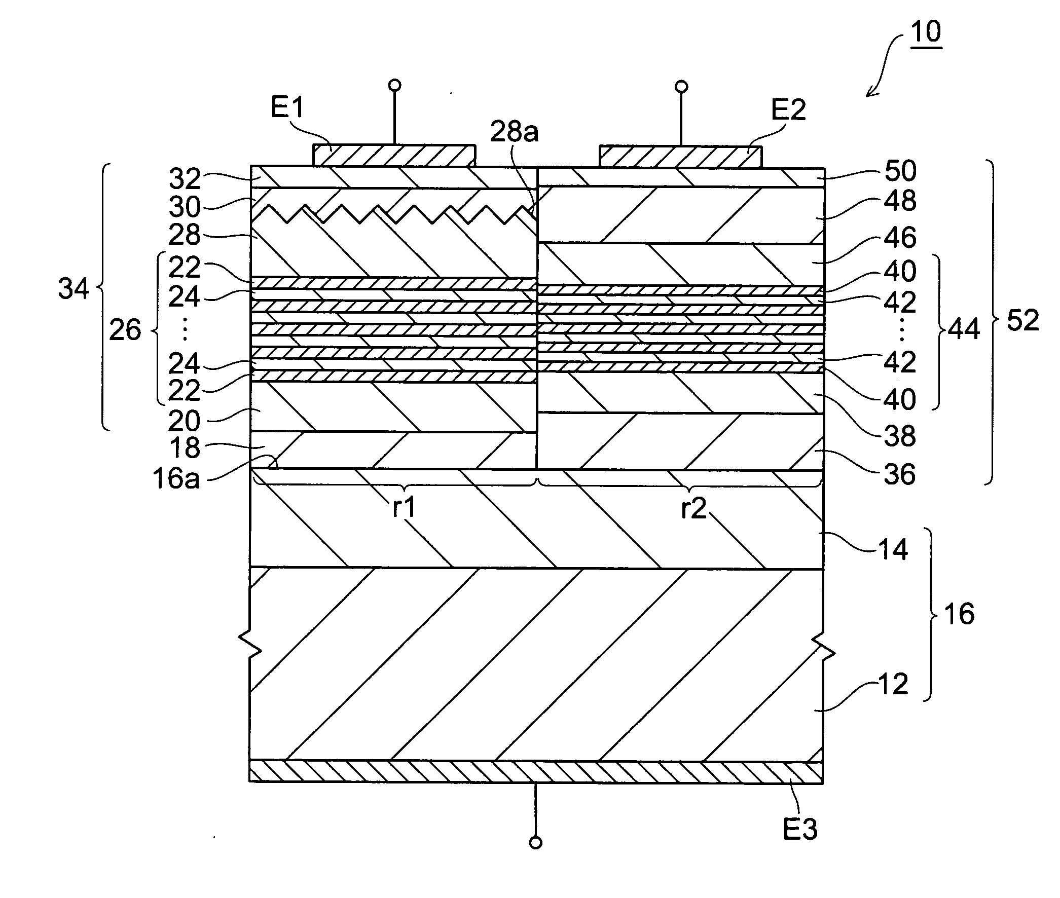
[0031]FIG. 1 is a cross-sectional view that schematically shows an example of an integrated optical device according to the The integrated optical device 10 shown in FIG. 1 comprises a first semiconductor optical element 34 that is provided on a first region r1 of a main face 16a of a substrate 16 and a second semiconductor optical element 52 that is provided on a second region r2 of the main face 16a of substrate 16. The semiconductor optical element 52 is optically coupled to semiconductor optical element 34. Therefore, the integrated optical device 10 has a butt joint structure. Further, a III-V compound semiconductor layer 18 including Al element is provided between substrate 16 and the semiconductor optical element 34. Electrodes E1 and E2 are each provided on the semiconductor optical element 34 and semiconductor optical element 52. An electrode E3 is provided on the underside of the substrate 16.
[0032] Substrate 16 comprises a substrate main body 12 and a buffer layer 14 whi...
second embodiment
[0058]FIG. 5 is a cross-sectional view that schematically shows an example of an integrated optical device according to the The integrated optical device 110 shown in FIG. 5 comprises a first semiconductor optical element 134 that is provided on a first region r1 of main face 16a of the substrate 16 and a second semiconductor optical element 152 that is provided on a second region r2 of main face 16a of substrate 16. The semiconductor optical element 152 is optically coupled to the semiconductor optical element 134. Therefore, the integrated optical device 110 has a butt joint structure. Further, a III-V compound semiconductor layer 118 containing Al element is provided between the substrate 16 and semiconductor optical element 134. Electrodes E1 and E2 are each provided on the semiconductor optical element 134 and semiconductor optical element 152. Electrode E3 is provided on the underside of the substrate 16.
[0059] The semiconductor optical element 134 comprises an optical confin...
PUM
 Abstract
Description
Claims
Application Information