Advanced Thin Flexible Microelectronic Assemblies and Methods for Making Same

a technology of microelectronic assemblies and thin strips, applied in the direction of basic electric elements, electrical equipment, semiconductor devices, etc., can solve the problems of microelectronic package and assembly to become smaller, not just in footprint, and dies to be thinned using a rather laborious grinding, polishing and etching process

Inactive Publication Date: 2008-01-10
THE JOHN HOPKINS UNIV SCHOOL OF MEDICINE
View PDF6 Cites 16 Cited by
  • Summary
  • Abstract
  • Description
  • Claims
  • Application Information

AI Technical Summary

Benefits of technology

[0013] Therefore, the present invention has been made in view of the above problems, and it is an objective of the present invention to provide ultra thin (

Problems solved by technology

As noted above, as technology has advanced, the standard glass fiber reinforced organic board has given way to unreinforced organic circuit boards, again causing reliability concerns.
Growing economic and application pressures have also forced microelectronic packages and assemblies to become smaller, not just in footprint, but also in height.
Currently, to accomp

Method used


Image

  • Advanced Thin Flexible Microelectronic Assemblies and Methods for Making Same
  • Advanced Thin Flexible Microelectronic Assemblies and Methods for Making Same
  • Advanced Thin Flexible Microelectronic Assemblies and Methods for Making Same

Examples


Embodiment Construction

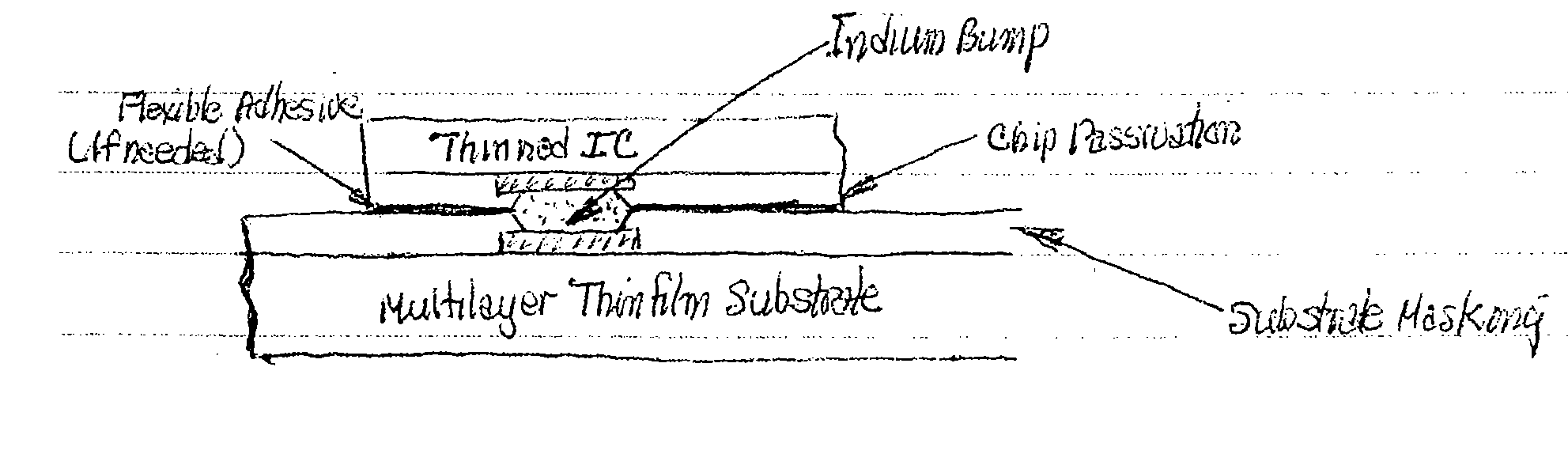
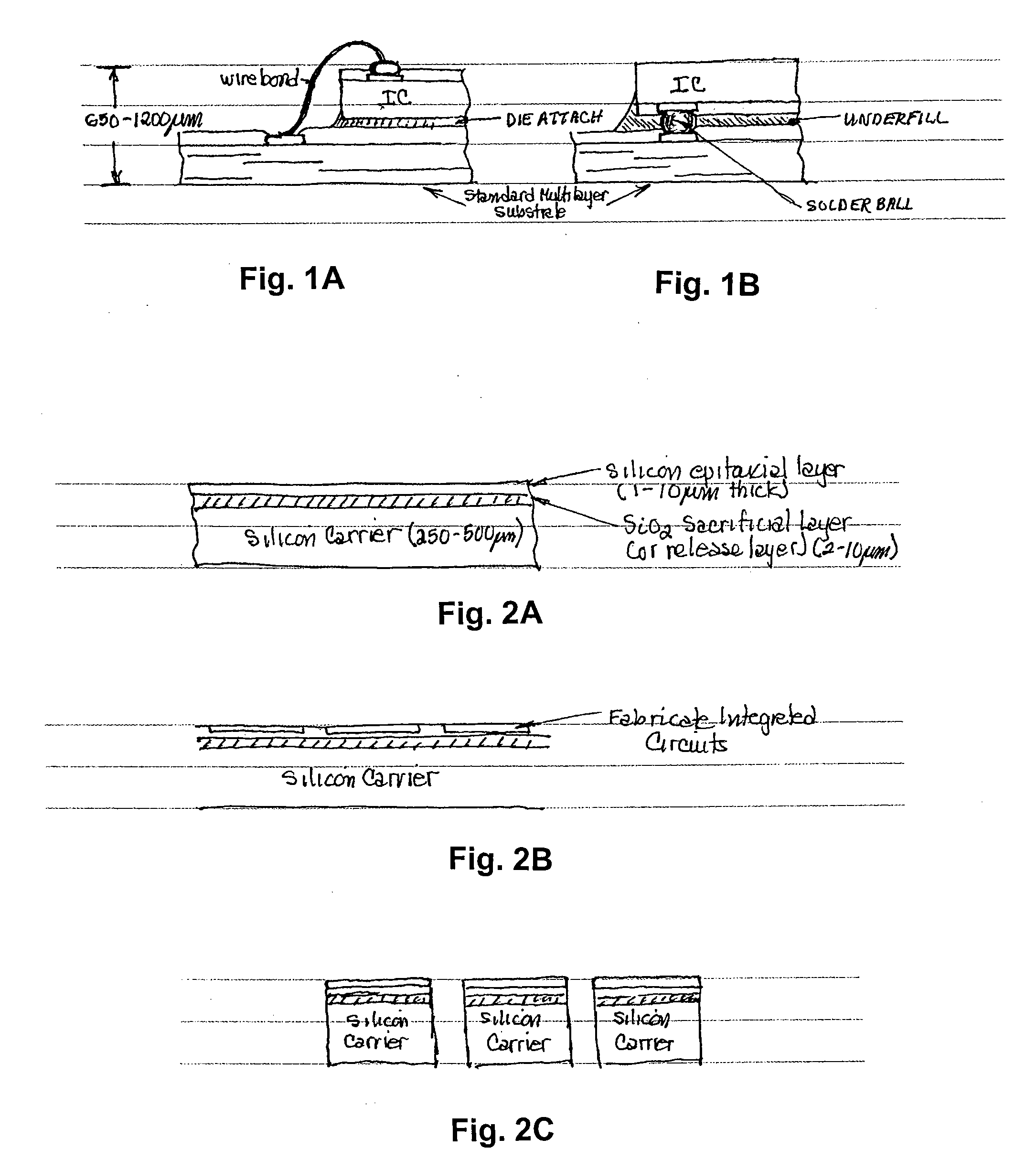
[0025] The method of the invention is capable of producing thinned die down to a thickness of 1 μm and routinely at the 5-10 μm level. In this technique, as shown in FIG. 2A, the die must be fabricated on a silicon on isulator wafer or carrier.

[0026] As also shown in FIG. 2A, a silicon epitaxial (Epi) layer of, for example, 1-10 μm in thickness is grown or deposited on a sacrificial or release layer of, for example, a 2-10 μm layer of an adhesive or oxide or nitride. By way of example only, FIG. 2A illustrates a deposit / growth of silicon dioxide (SiO2) on a silicon wafer or carrier. The integrated circuit process then takes place in the standard manner with the creation of integrated circuits in the Epi layer (FIG. 2B). The sacrificial layer of, e.g., SiO2 (oxide layer) and the silicon carrier serve as a backside handle. Once the integrated circuit creation process is completed, the Epi can be bumped, as appropriate, while still attached to the oxide layer-carrier. The die can then...


PUM


Abstract

A thin, flexible microelectronic assembly using thinned die (5-10 microns and lower) produced by growing a 1 μm-10 μm silicon epitaxial (Epi) layer on an oxidized silicon carrier. The integrated circuit process takes place in the standard manner in the Epi layer. The oxide layer and the silicon carrier serve as the backside handle. Once processed, the wafer can be bumped and singulated just like a normal chip without the need for the extra handle attachment processes or the backside thinning operation. Once the integrated circuits are flipped and solder reflowed to a substrate, the handle can be removed by etching the oxide. In one assembly embodiment, wells are etched in the flexible circuit board material to allow the interconnect to be recessed below the circuit board surface. An adhesive can then be placed on the board surface, locking the die to the flexible substrate. Alternatively, a nanowire interposer can be sandwiched between a bumped multilayer substrate and a bumped thin die. Further, indium bumps can be substituted for solder bumps to provide a more flexible assembly.

Description

CROSS REFERENCE TO RELATED APPLICATIONS [0001] This application claims the benefit of prior filed, co-pending U.S. provisional application: Ser. No. 60 / 809,874, filed on Jun. 1, 2006, which is incorporated herein by reference in its entirety.BACKGROUND OF THE INVENTION [0002] 1. Field of the Invention [0003] The present invention relates generally to microelectronic packaging and, more particularly, to advanced thin flexible microelectronic assemblies and methods for making such assemblies. [0004] 2. Description of the Related Art [0005] Conventional microelectronic packaging involves the mounting of standard integrated circuit die in either a face-up (wirebonded) or a face-down (flip chip) configuration as shown in FIGS. 1A and 1B, respectively. Techniques for implementing such configurations are well known and have been reported in the literature for almost 50 years. [0006] Initially, such mounting took place on substrates with matched coefficients of thermal expansion (CTE) such ...

Claims


Application Information

Patent Timeline
IPC IPC(8): H01L21/70
CPCH01L21/6835H01L24/83H01L2924/10253H01L2924/0665H01L2924/014H01L2924/01033H01L2224/2919H01L2924/14H01L2924/01049H01L2924/01029H01L2224/83851H01L2224/838H01L2224/73265H01L2224/73204H01L2224/48465H01L2224/48227H01L2224/48091H01L2224/32225H01L2224/29499H01L2224/16225H01L2221/6835H01L2221/68345H01L24/90H01L2924/00014H01L2924/00H01L2924/00012H01L24/73H01L2224/05567H01L2224/0557H01L2224/05573H01L2224/05571H01L2224/0554H01L2224/05599H01L2224/0555H01L2224/0556
Inventor CHARLES, HARRY K. JR.BANDA, CHARLES V.FRANCOMACARO, ARTHUR S.KEENEY, ALLEN C.LEHTONEN, SEPPO J.
Owner THE JOHN HOPKINS UNIV SCHOOL OF MEDICINE
Why Eureka
Try Eureka