

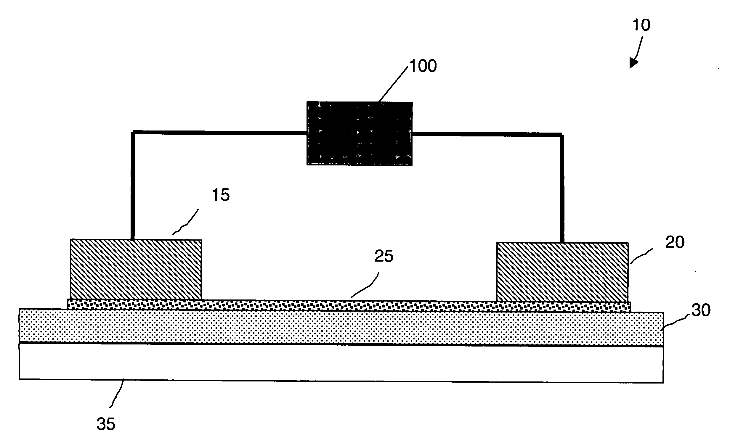
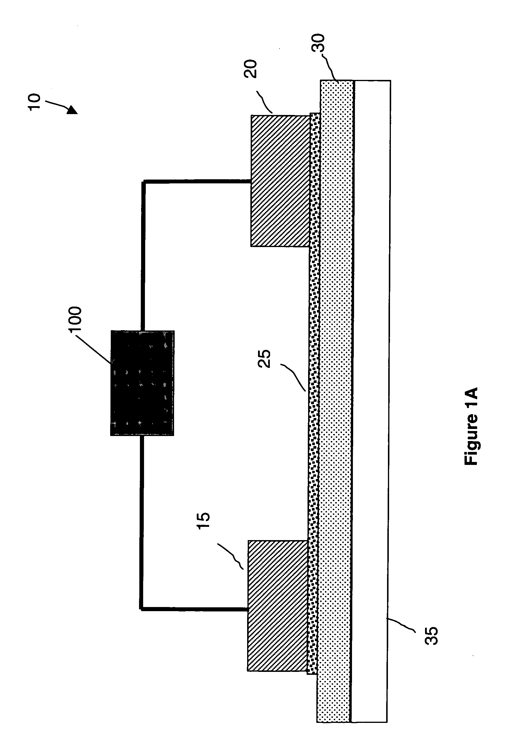
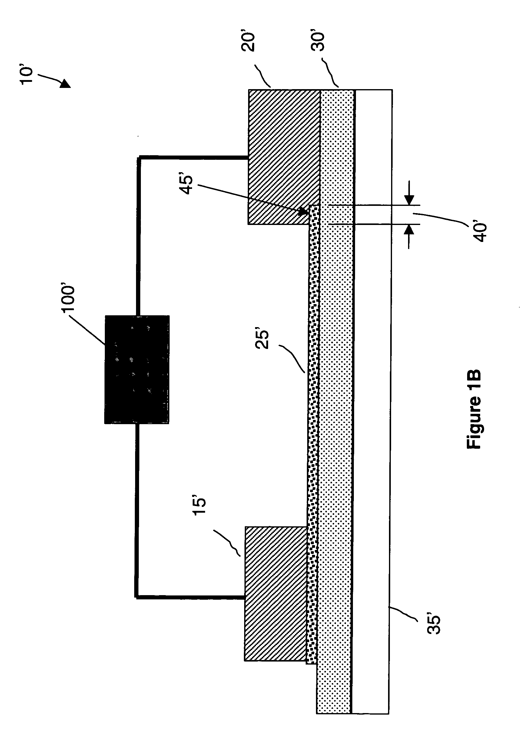
Two-terminal nanotube devices and systems and methods of making same
a technology of nanotubes and terminals, applied in the field of switching devices, can solve the problems of high power consumption, density and operating speed of mos digital circuits, and limited density of bipolar digital integrated circuits, and achieve the effects of minimizing heat flow, and minimizing heat flow out of nanotube elements
- Summary
- Abstract
- Description
- Claims
- Application Information
AI Technical Summary
Benefits of technology
Problems solved by technology
Method used
Image

Examples
example fabrication
[0261] Example Fabrication Procedure
[0262] An initial structure consists of a 4″ Si wafer with a layer of 30 nm of thermal SiO2. A set of gold alignment marks is patterned on the wafer to define an array of 60 die measuring 7 mm square. The wafer is pre-treated with an oxygen plasma for 2 min using an O2 asher. 3 ml of aqueous nanotube solution containing a majority of MWNTs (greater than 50%) and SWNTs, (and bundles thereof), is dispensed onto the oxide layer of a Si wafer. A fabric of nanotubes is applied via a spin coating process which is more fully described in incorporated references. The wafer is baked on a hotplate at 150 C after the nanotube spin coat, and the sheet resistance of the resulting nanofabric is measured by 4-point probe. This nanotube deposition procedure is repeated until the sheet resistance of the nanofabric is below a specified value of about 1-2 kΩ. The wafer is baked on a hotplate at 150 C between and after the nanotube spin coats.
[0263] 400 nm of PMMA r...
PUM
 Abstract
Description
Claims
Application Information