Semiconductor integrated circuit

a technology of integrated circuits and semiconductors, applied in pulse manipulation, pulse technique, instruments, etc., can solve the problems of reducing the operating speed reducing the reproducing quality of the class-d amplifier, and sacrificing the load or the class-d amplifier. , to achieve the effect of reducing the ringing

Inactive Publication Date: 2008-01-17
YAMAHA CORP
View PDF8 Cites 9 Cited by
  • Summary
  • Abstract
  • Description
  • Claims
  • Application Information

AI Technical Summary

Benefits of technology

[0008] According to the invention, when ringing occurs in the output signal due a switching operation of the output buffer circuit to and the output signal exceeds the reference level in the positive or negative direction, the switching element is turned on. As a result, a discharge occurs from the output signal line to the low-potential power line or the high-potential power line and the ringing is thereby reduced.

Problems solved by technology

Therefore, a noise is generated on these parasitic inductances, resulting in a ringing which appears in an output signal of the class-D amplifier.
Such a ringing causes a deterioration in reproducing quality of the class-D amplifier, and furthermore, causes a damage to the load or the class-D amplifier.
For this reason, there is a problem in that an operating speed of the class-D amplifier is sacrificed by the application of the technique.
This problem is common to a semiconductor integrated circuit required to drive a load at a high speed and demanded to reduce a ringing in an output signal in addition to the class-D amplifier.

Method used


Image

  • Semiconductor integrated circuit
  • Semiconductor integrated circuit
  • Semiconductor integrated circuit

Examples


embodiment 1

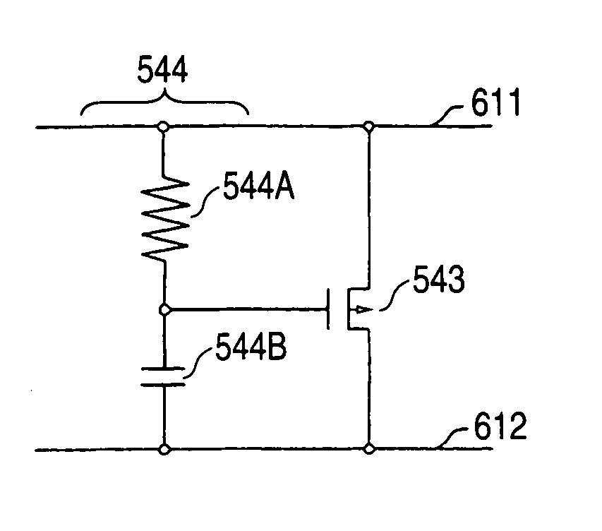
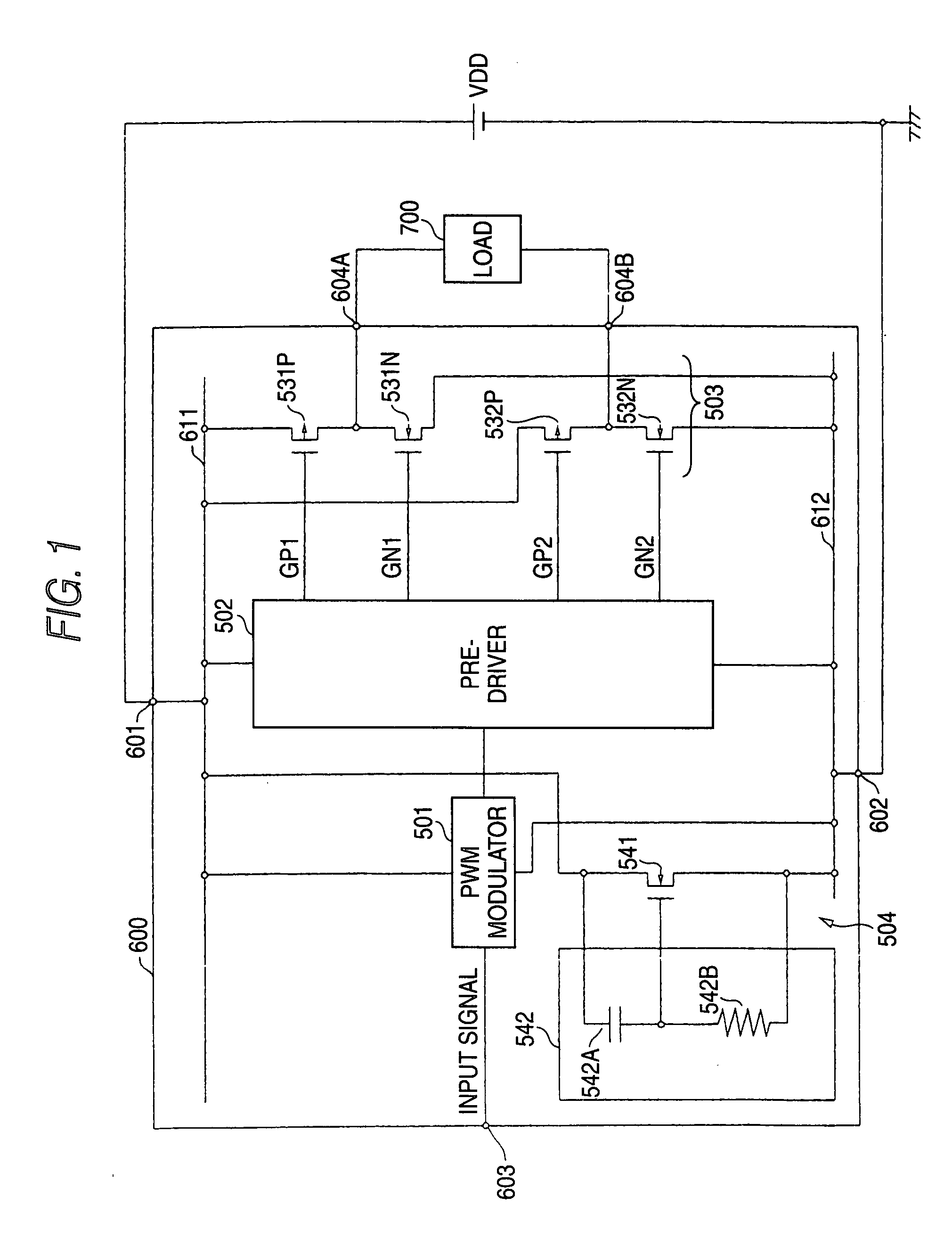
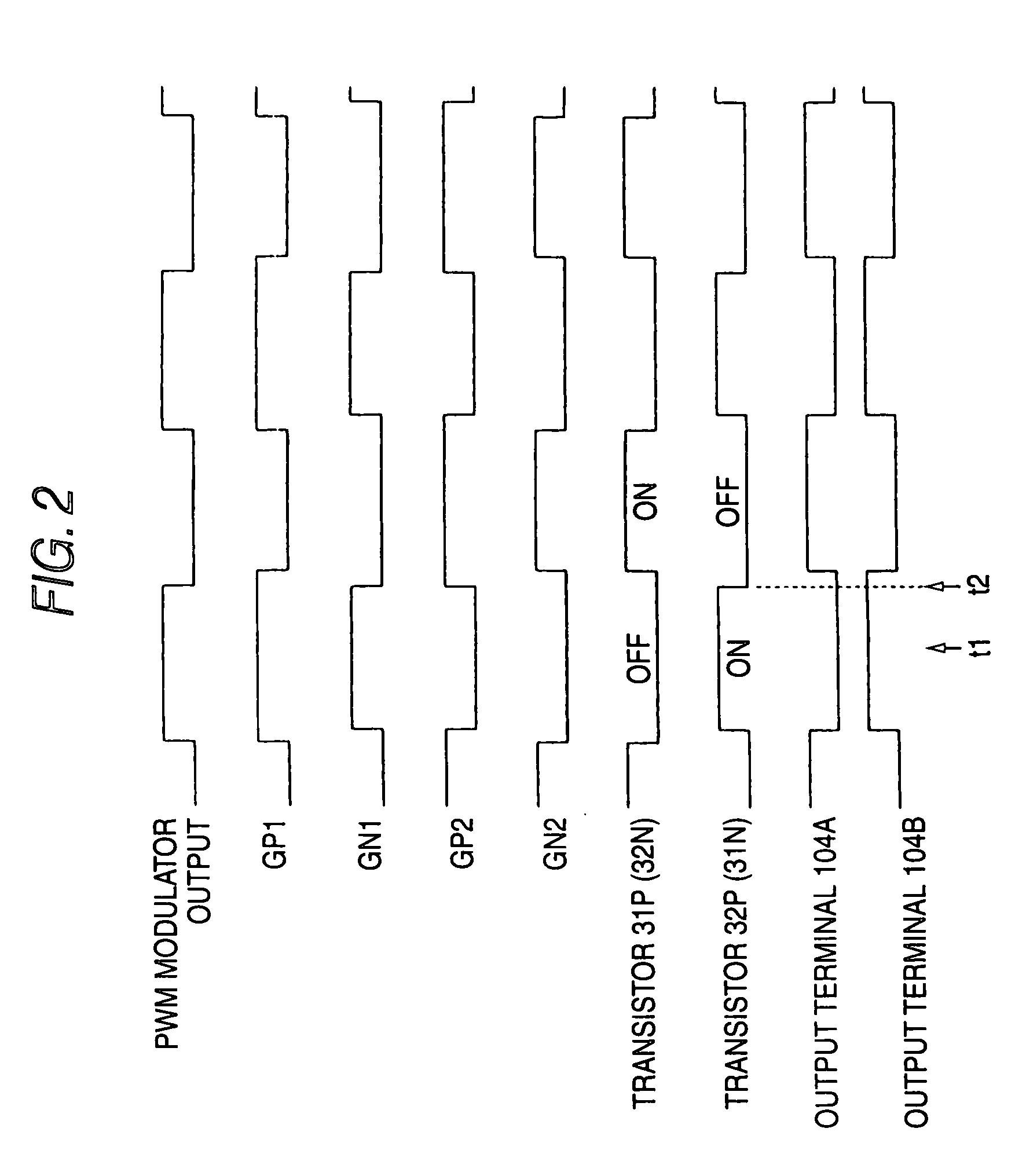
[0022]FIG. 1 is a circuit diagram showing a structure of a class-D amplifier 600 according to an embodiment 1 of a semiconductor integrated circuit in accordance with the invention. The class-D amplifier 600 has a high potential power terminal 601, a low potential power terminal 602, an input terminal 603, and output terminals 604A and 604B. The high potential power terminal 601 is connected to a positive electrode of a power supply VDD, and the low potential power terminal 602 is connected to a negative electrode of the power supply VDD and is grounded. In an example shown in the drawing, a single power supply is used. For this reason, the low potential power terminal 602 is grounded. In the case in which there is employed such a structure that a power supply for generating a positive source voltage and a power supply for generating a negative source voltage are used, however, it is preferable that the high potential power terminal 601 should be connected to an output terminal of t...

embodiment 2

[0033]FIGS. 6 and 7 are circuit diagrams showing the configuration of a class-D amplifier 100A having ringing reduction circuits 40NA and 40PA according to an embodiment 2 of the invention. FIG. 6 shows the circuit configuration of the ringing reduction circuit 40NA and FIG. 7 shows the circuit configuration of the ringing reduction circuit 40PA.

[0034] The class-D amplifier 100A has a high-potential power terminal 101, a low-potential power terminal 102, an input terminal 103, and an output terminal 104. The high-potential power terminal 101 is connected to the positive pole of a power source VDD via a high-potential power line 131 disposed outside the class-D amplifier 100A, and the low-potential power terminal 102 is connected to the negative pole of the power source VDD via a low-potential power line 132 disposed outside the class-D amplifier 100A and is grounded. In the illustrated example, the low-potential power terminal 102 is grounded because of the use of the single power ...

embodiment 3

[0045]FIGS. 9 and 10 are circuit diagrams showing the configuration of a class-D amplifier 100B having ring reduction circuits 40PB and 40NB according to an embodiment 3 of the invention. FIG. 9 shows the circuit configuration of the ringing reduction circuit 40NB and FIG. 10 shows the circuit configuration of the ringing reduction circuit 40PB. In FIGS. 9 and 10, components having corresponding components in FIGS. 6 and 7 referred to above are given the same reference symbols as the latter and will not be described.

[0046] In the embodiment 2, the comparators 410 and 420 which are the ringing detector detect occurrence of ringing in the output signal OUT by comparing the level of the output signal line 120 with the level PVDDI of the high-potential power line 111 or the level PVSSI of the low-potential power line 112.

[0047] However, when a switching current of the output buffer circuit 30 flows through the parasitic inductance 141 or 142, a large counterelectromotive force is indu...


PUM


Abstract

An N-channel transistor is provided as a switch between a high potential power line and a low potential power line. A high-pass filter is constituted by a capacitor and a resistor. When a voltage between the high potential power line and the low potential power line is started to oscillate by a switching operation, the high-pass filter causes a high-pass component thereof to pass, thereby turning ON the N-channel transistor to reduce a ringing.

Description

BACKGROUND OF THE INVENTION [0001] The present invention relates to a semiconductor integrated circuit and more particularly to a semiconductor integrated circuit which is suitable for a circuit for pulse driving a load such as a class-D amplifier. [0002] As is well known, a class-D amplifier serves to turn ON / OFF a load driving output transistor and to intermittently carry out a conduction to a load. In the intermittent conduction to the load, a current flowing to parasitic inductances provided on a power line or a grounding conductor of the class-D amplifier is drastically changed. Therefore, a noise is generated on these parasitic inductances, resulting in a ringing which appears in an output signal of the class-D amplifier. Such a ringing causes a deterioration in reproducing quality of the class-D amplifier, and furthermore, causes a damage to the load or the class-D amplifier. For this reason, it is desired to reduce the ringing. Patent Document 1 has proposed a technique for ...

Claims


Application Information

Patent Timeline
Patent Type & Authority Applications(United States)
IPC IPC(8): H04B1/10
CPCH03F3/217G11C7/10H01L29/417H01L29/772
Inventor TSUJI, NOBUAKIKAWAI, HIROTAKA
Owner YAMAHA CORP
Why Eureka
Try Eureka