Structure and method of fabricating a hinge type MEMS switch

a technology of hinge type and switch, applied in the direction of magnets, relays, magnetic bodies, etc., can solve the problems of no reference, design also requires a relatively high voltage, and the inability to restore the switch to its original sta

Inactive Publication Date: 2008-01-17
INT BUSINESS MASCH CORP
View PDF8 Cites 50 Cited by
  • Summary
  • Abstract
  • Description
  • Claims
  • Application Information

AI Technical Summary

Benefits of technology

[0019] The MEMS switch of the present invention is easily integrated in an IC chip. All the elements forming the switching device are fabricated using semiconductor back-end-of-the-line (or BEOL) process, and as such, these switches can easily be manufactured alongside other semiconductor devices and circuits on the same substrate.
[0021] Another aspect of the invention provides a method of fabricating a MEMS switch on a substrate that includes the steps of: i) forming at least one depletion area within the substrate, followed by a blanket deposition of an etch stop layer thereon; ii) depositing a first metallization layer on the substrate followed by a first dielectric layer, and patterning the first metal layer with a first portion of the metal residing within the depletion and a second portion thereof residing outside the depletion area, and patterning the first dielectric layer, leaving dielectric only on top of the metal residing within the depletion area, forming at the first metallization layer: a) bases for hinge posts, b) lower electrodes and c) lower interconnect wiring; iii) blanket depositing and planarizing a second dielectric layer deposited thereon, to form conductive vias in areas where interconnects are expected, the vias becoming a first portion of hinges; iv) depositing a second dielectric layer a second metallization layer followed by patterning to form: a) the lower electrodes, b) links to upper electrodes to be formed thereafter, c) a rigid movable conductive plate with holding rings on two opposing edges of the rigid movable conductive plate, and d) a second portion of the hinge posts; v) blanket depositing a third dielectric layer thereon followed by patterning, forming conductive vias in areas where interconnects are expected to become the third portion of the hinges, and interconnect wiring to provide links to the upper electrodes to be formed thereafter; vi) depositing a fourth dielectric layer, followed by a deposition a third metallization layer thereon, and patterning to form: a) upper hinge caps, b) the upper electrodes, and c) upper interconnect wiring; and vii) depositing a fifth dielectric serving as a hard mask, and opening a cavity down to the etch stop layer to allow the conductive plate to move freely.

Problems solved by technology

Such devices, however, present many problems because their structure and innate material properties require that they be manufactured in lines that are separate from conventional semiconductor manufacture processing.
This is usually due to materials and processes which are incompatible and which cannot be integrated within existing semiconductor fabrication lines.
However, it must be provided with a low actuation-voltage switch and must not suffer from stiction, that is, the inability to restore the switch to its original state when desired.
This design also requires a relatively high voltage.
Furthermore, the process steps to fabricate a hinge-type MEMS switch are not described by Feng et al., and no reference is made on how to integrate this type of MEMS switches alongside with back-end-of-the-line (BEOL) metal interconnects of a conventional semiconductor chip.
In order to change the state of the switch, each time 20 mA current must be applied, which is not practical for a CMOS chip environment.
High-currents of this magnitude are not suitable for CMOS applications.
To date, conventional MEMS switches are not CMOS compatible because: (1) they are difficult to integrate using MOS process steps and, (2) they require a high-current and high actuation operation voltages.

Method used


Image

  • Structure and method of fabricating a hinge type MEMS switch
  • Structure and method of fabricating a hinge type MEMS switch
  • Structure and method of fabricating a hinge type MEMS switch

Examples


Embodiment Construction

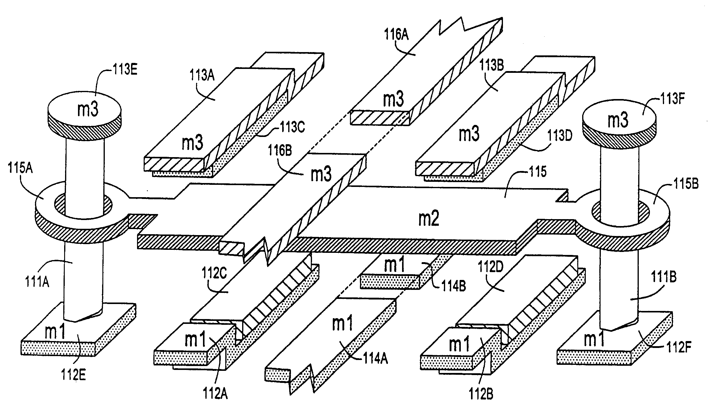
[0030] Referring now to the drawings and, more particularly, to FIG. 4 there is shown a three dimensional view of the hinge-type switch of the present invention.

[0031] As previously described, the MEMS switch is activated by a low actuation voltage, which has the advantage of making the switch compatible with voltages that are characteristic of semiconductor devices, in particular CMOS technology. This is made possible by the device not having to rely on a deformable moveable beam, that is typical of, e.g., cantilever MEMS switching devices and the like.

[0032] Still referring to FIG. 4, the structure is shown consisting of two guiding posts 111A and 111B, each formed by a column terminating, respectively, in a bottom and a top cap. The top cap is made of third metal (m3), preferably, having a size approximately 50% larger than the cross-sectional area of the column forming the post. The bottom cap is made of first metal (m1), which size, preferably, approximates the size of the to...


PUM

PropertyMeasurementUnit
operating voltageaaaaaaaaaa
actuation voltageaaaaaaaaaa

Abstract

A hinge type MEMS switch that is fully integratable within a semiconductor fabrication process such as a CMOS, is described. The MEMS switch constructed on a substrate consists of two posts, each end thereof terminating in a cap; a rigid movable conductive plate having a surface terminating in a ring in each of two opposing edges, the rings being loosely connected to guiding posts; upper and lower electrode pairs; and upper and lower interconnect wiring lines connected and disconnected by the rigid movable conductive plate. When in the energized state, a low voltage level is applied to the upper electrode pair, while the lower electrode pair is grounded. The conductive plate moves up, shorting two upper interconnect wirings lines. Conversely, the conductive plate moves down when the voltage is applied to the lower electrode pair, while the upper electrode pair is grounded, shorting the two lower interconnect wiring lines and opening the upper wiring lines. The MEMS switch thus formed generates an even force that provides the conductive plate with a translational movement, with the displacement being guided by the two vertical posts.

Description

CROSS REFERENCE TO RELATED PATENTS [0001] This application is a divisional of U.S. patent application Ser. No. 10 / 905,449, filed on Jan. 5, 2005.BACKGROUND OF THE INVENTION [0002] This invention generally relates to micro-electromechanical system (MEMS) switches, and more particularly, to a hinge type MEMS switch and a method of fabricating the same using current state of the art semiconductor fabrication processes, such as a CMOS process. [0003] Switching operations are a fundamental part of many electrical, mechanical and electromechanical applications. MEMS switches have drawn considerable interest over the last few years, leading to the design and development of a variety of products using MEMS technology that have become widespread in biomedical, aerospace, and communications systems applications. [0004] Conventional MEMS typically utilize cantilever switches, membrane switches, and tunable capacitor structures, as described, e.g., in U.S. Pat. No. 6,160,230 to McMillan et al.,...

Claims


Application Information

Patent Timeline
Patent Type & Authority Applications(United States)
IPC IPC(8): H01L21/00
CPCH01H1/20H01H59/0009H01H2001/0084H01H2001/0089Y10T29/49208Y10T29/49155Y10T29/49105Y10T29/49204Y10T29/49128
Inventor HSU, LOUISDALTON, TIMOTHYCLEVENGER, LAWRENCERADENS, CARLWONG, KWONG HONYANG, CHIH-CHAO
Owner INT BUSINESS MASCH CORP
Why Eureka
Try Eureka