

LED packaging structure
- Summary
- Abstract
- Description
- Claims
- Application Information
AI Technical Summary
Benefits of technology
Problems solved by technology
Method used
Image

Examples
Embodiment Construction
[0017]The following description is of the best presently contemplated mode of carrying out the present invention. This description is not to be taken in a limiting sense but is made merely for the purpose of describing the general principles of the invention. The scope of the invention should be determined by referencing the appended claims.
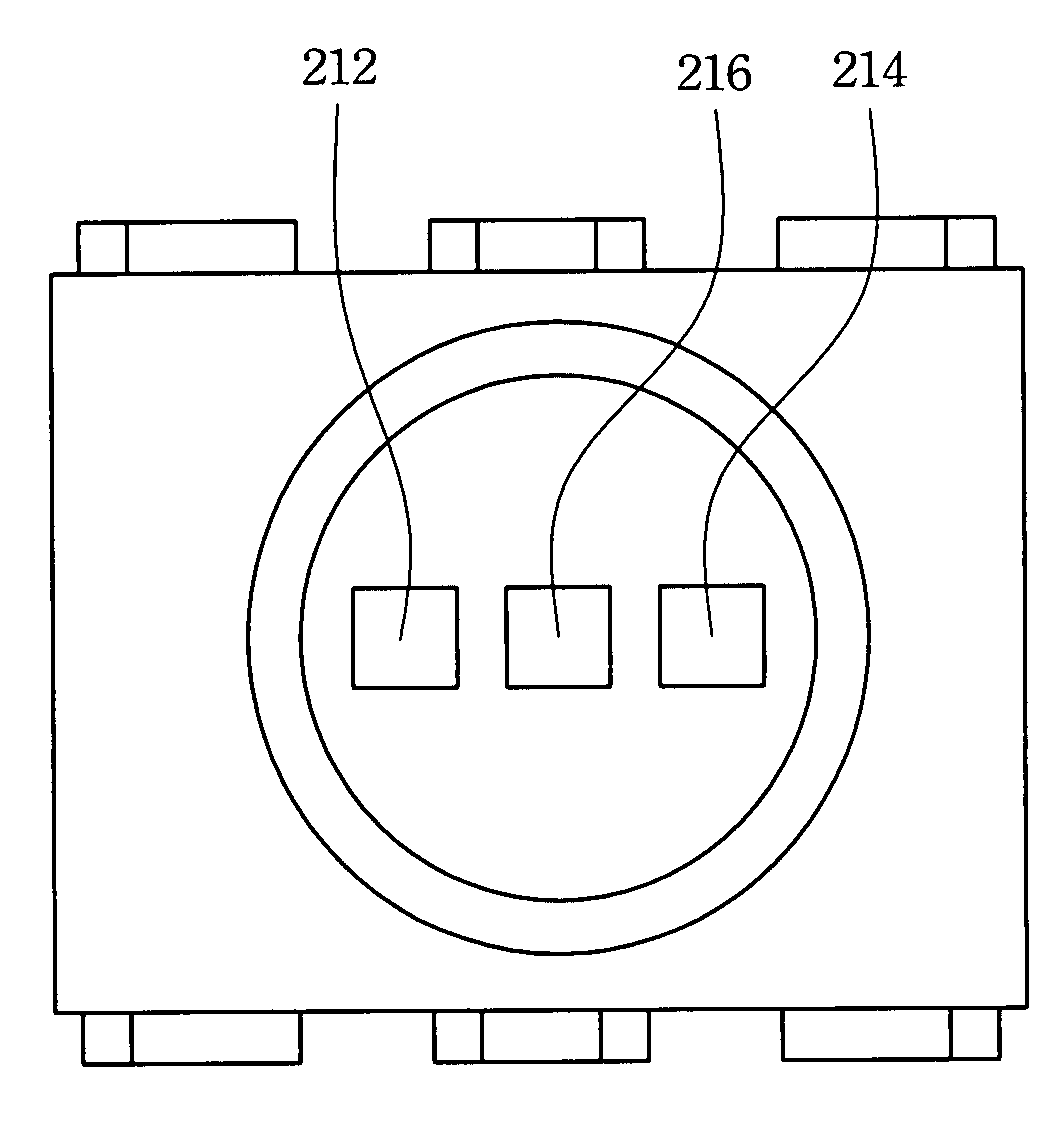
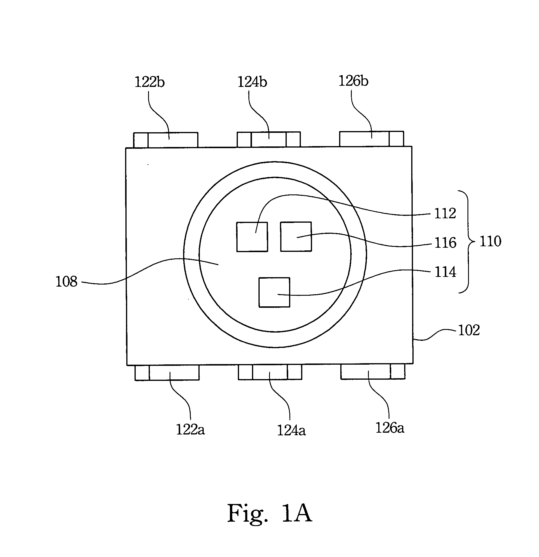
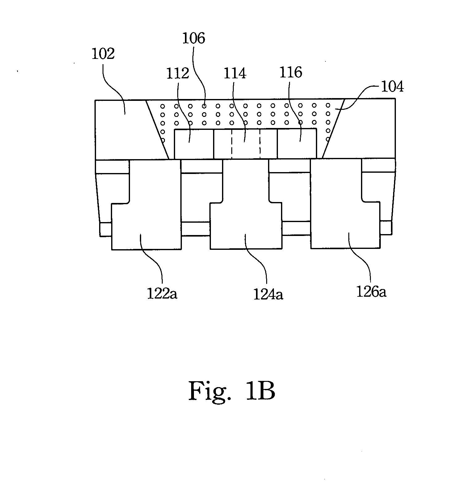
[0018]Referring to FIGS. 1A and 1B, a top view and a side view of a preferred embodiment of the light emitting diode packaging structure according to the present invention are respectively illustrated. Additionally, the package material 104 is omitted from FIG. 1A to clearly present the accommodating room 108.
[0019]In one embodiment, the light emitting diode packaging structure includes a package body 102, an LED chipset 110, a package material 104, a phosphor 106 and electrode leads.
[0020]The package body 102 is injected and formed by the materials of polyphthalamide (PPA), epoxy resin, glass fiber, calcium oxide and so on. The package body 102 ...
PUM
 Abstract
Description
Claims
Application Information