A high-efficiency thin-film photovoltaic cell
A thin-film photovoltaic cell, high-efficiency technology, applied in photovoltaic power generation, circuits, electrical components, etc., can solve problems such as low efficiency and excessively wide band gap of amorphous silicon materials, achieve low process cost, improve light absorption efficiency, reduce silicon the effect of consumption
- Summary
- Abstract
- Description
- Claims
- Application Information
AI Technical Summary
Problems solved by technology
Method used
Image
Examples
Embodiment 1
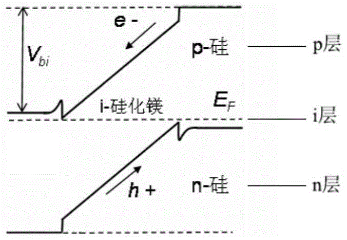
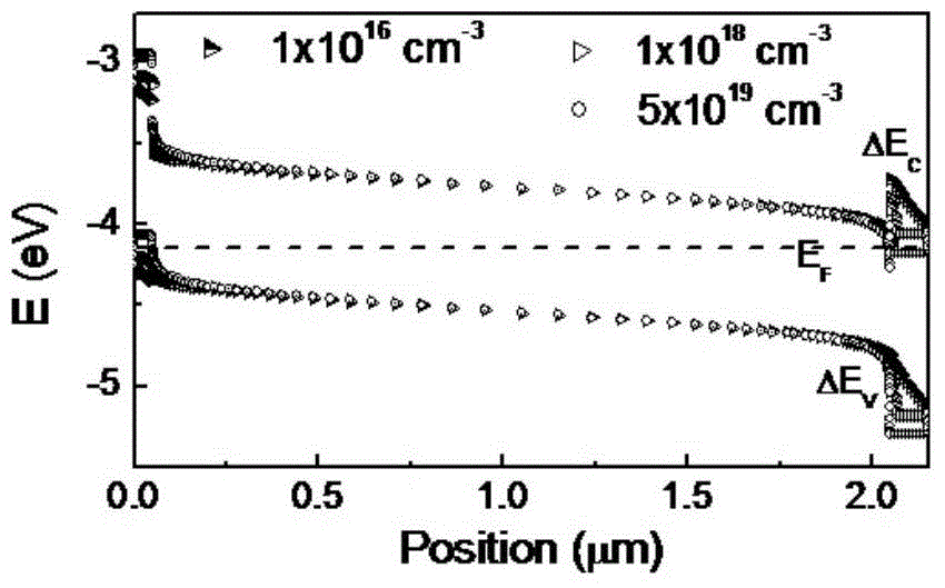
[0036] The schematic diagram of the structure of the high-efficiency thin-film photovoltaic cell in this embodiment is as follows figure 1 As shown, it includes a top electrode layer 1 made of n-type transparent conductive oxide and a back ohmic contact electrode layer 5, and a p-i-n junction layer is arranged between the top electrode layer 1 and the back ohmic contact electrode layer 5, and the p-i-n junction The layers include heavily doped n-type silicon light absorbing layer 2 , magnesium silicide light absorbing layer 3 and heavily doped p-type silicon light absorbing layer 4 . Among them, the top electrode is a commercially available FTO electrode; the heavily doped p-type silicon light absorbing layer 4 is made of heavily doped polysilicon (the doping element is phosphorus), the thickness is 0.05 microns, and the carrier concentration is 5×10 18 cm -3 ; Magnesium silicide photoabsorbing layer 3 adopts intrinsic magnesium silicide, with a thickness of 2 microns and a c...
Embodiment 2
[0045] The high-efficiency thin-film photovoltaic cell in this embodiment includes a top electrode layer and a back ohmic contact electrode layer made of n-type transparent conductive oxide, and an n-i-p junction layer is arranged between the top electrode layer and the back ohmic contact electrode layer. The n-i-p junction layer includes a heavily doped n-type silicon light absorbing layer, a magnesium silicide light absorbing layer and a heavily doped p-type silicon light absorbing layer. Among them, the top electrode layer is a commercially available AZO electrode, and the heavily doped n-type silicon light absorbing layer is made of heavily doped polysilicon (doped with phosphorus), with a thickness of 0.05 microns and a carrier concentration of 5×10 18 cm -3 , the magnesium silicide photoabsorbing layer adopts intrinsic magnesium silicide, the thickness is 2000 nm, and the carrier concentration is 10 17 cm -3 , the heavily doped p-type silicon layer is made of heavily d...
Embodiment 3
[0053] The high-efficiency thin-film photovoltaic cell in this embodiment includes a top electrode layer and a back ohmic contact electrode layer made of n-type transparent conductive oxide, and a p-i-n junction layer is arranged between the top electrode layer and the back ohmic contact electrode layer. The p-i-n junction layer includes a heavily doped p-type amorphous silicon light absorbing layer, a magnesium silicide light absorbing layer and a heavily doped p-type amorphous silicon light absorbing layer. Among them, the top electrode layer adopts commercially available ITO electrodes; the p-type silicon photosensitive absorption layer adopts heavily doped amorphous silicon (doped element boron), with a thickness of 0.05 microns and a carrier concentration of 5×10 20 cm -3 ; The magnesium silicide photoabsorbing layer is made of intrinsic magnesium silicide, with a thickness of 2 microns and a carrier concentration of 10 12 cm -3 ; The n-type silicon light absorbing laye...
PUM
 Abstract
Description
Claims
Application Information


