Constant Voltage Generating Circuit

a constant voltage generation and circuit technology, applied in amplifiers, amplifiers with semiconductor devices/discharge tubes, instruments, etc., can solve problems such as malfunctions, not giving full stability in some cases, and increasing current consumption at start time, so as to increase the amount, quick stabilize the output potential, and quick stabilize

Active Publication Date: 2008-01-24
CITIZEN WATCH CO LTD
View PDF13 Cites 3 Cited by
  • Summary
  • Abstract
  • Description
  • Claims
  • Application Information

AI Technical Summary

Benefits of technology

[0039] The present invention solves the problems with the prior art described above. It is an object of the present invention to provide a constant voltage generating circuit that provides an output potential that is stable against power supply voltage variations without being affected by power supply variations, provides good startability from the time the power is turned on to the time the potential becomes stable, and outputs a stable regulated voltage shortly after the power is turned on.
[0040] It is another object of the present invention to provide a simple circuit configuration, which eliminates the need for an additional circuit such as the switching control means, to gain output potential stability against the power supply voltage variations described above and to ensure good startability from the time the power is turned on to the time the potential becomes stable.
[0041] It is still another object of the present invention to provide a circuit configuration that can produce a stable regulated voltage shortly after the power is turned on without worrying about the noises and the current resistance characteristics.

Problems solved by technology

Therefore, when the constant voltage generating circuit shown in FIG. 8 is used as the power supply of an internal circuit, the problem is that the current consumption at start time increases because the regulated voltage VREG is almost equal to the power supply voltage.
When this constant voltage generating circuit is used as an analog-based bias power supply, the problem is that a malfunction may occur because an appropriate bias voltage cannot be supplied at least for the period T1.
However, a later study indicates that the invention described above has a problem with the output potential stability against power supply voltage variations, which is another requirement for the constant voltage generating circuit described above, and, as a result, does not give full stability in some cases.
Therefore, the output potential stability against the power supply variation is low.
On the other hand, the capacity of the capacitor 17, if decreased, can weaken the effect of the power supply variation, in which case, however, the system does not achieve the full effect of startability improvement.
However, the problem with the constant voltage circuit described above is that the switching control means 72 must be provided separately, because the circuit has a configuration in which the on / off state of the switching means 71 is controlled by means of the switching control means 72.
However, in this configuration where a large current flows in the switching control means 72 in a short period of time, there is a problem that the current resistance characteristics of the devices configuring the switching control means 72, as well as the noises generated in the switch current means, must be taken into consideration.

Method used


Image

  • Constant Voltage Generating Circuit
  • Constant Voltage Generating Circuit
  • Constant Voltage Generating Circuit

Examples


first embodiment

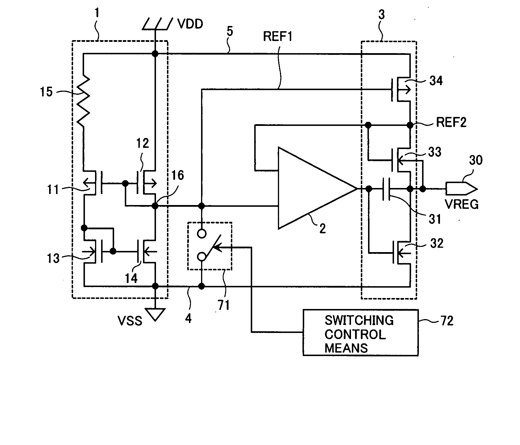
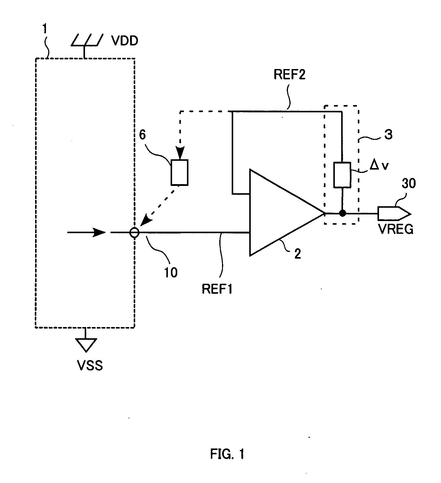
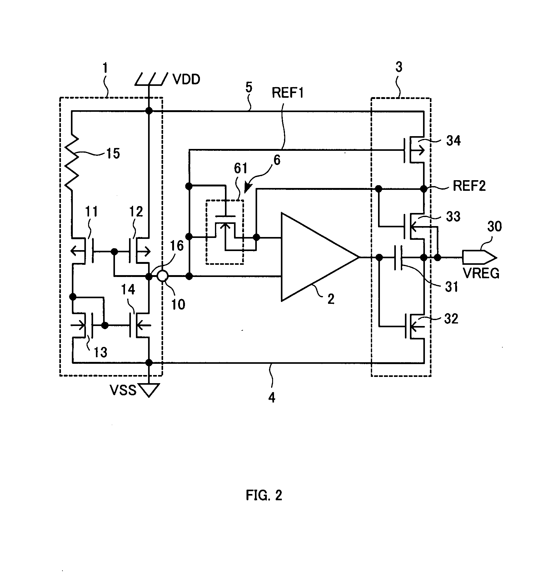
[0079]FIG. 2 is a circuit diagram showing the configuration of a constant voltage generating circuit in a first embodiment in which the output terminal of a voltage generation source is connected to another input terminal of a differential amplifier for a fixed period of time immediately after the power is turned on.

[0080] As shown in FIG. 2, switching means 6 in the first embodiment comprises an NMOS transistor 61, and the switching between the on-state and the off-state of this NMOS transistor 61 is controlled by the signal (potential entered into another input terminal of the differential amplifier) in the constant voltage generating circuit. Because the open / close state of the NMOS transistor 61 is controlled by the potential applied to the transistor, the first embodiment eliminates the need for the switching control means 72 that is included in the conventional configuration.

[0081] The gate and the drain of the NMOS transistor 61 are connected to an output node 16 (output te...

second embodiment

[0087]FIG. 4 is a circuit diagram showing the configuration of a constant voltage generating circuit in a second embodiment. As in the first embodiment, the output terminal of the voltage generation source is connected to another input terminal of the differential amplifier for a fixed period of time immediately after the power is turned on.

[0088] Switching means 6 in the second embodiment comprises a PMOS transistor 62 as shown in FIG. 4, and the switching between the on-state and the off-state of this PMOS transistor 62 is controlled by the signal (potential input to another input terminal of the differential amplifier) in the constant voltage generating circuit. The switching between the open / close state of the PMOS transistor 62 is controlled by the potential applied to the transistor and, so, the second embodiment also eliminates the need for the switching control means 72 that is required in the conventional configuration.

[0089] The source of the PMOS transistor 62 is connec...

third embodiment

[0095]FIG. 5 is a circuit diagram showing the configuration of a constant voltage generating circuit in a third embodiment, in which the output terminal of the voltage generation source is connected to the negative power supply line for a fixed period of time immediately after the power is turned on.

[0096] Switching means 6 in the third embodiment comprises a PMOS transistor 63 as shown in FIG. 5, and the switching between the on-state and the off-state of this PMOS transistor 63 is controlled by the signal (potential input to another input terminal of the differential amplifier) in the constant voltage generating circuit. The switching between the open / close state of the PMOS transistor 63 is controlled by the potential applied to the transistor and, so, the third embodiment also eliminates the need for the switching control means 72 that is required in the conventional configuration.

[0097] The source, the gate, and the drain of the PMOS transistor 63 are connected, respectively,...


PUM


Abstract

A constant voltage generating circuit according to the present invention includes a reference voltage generation source 1, a differential amplifier 2 that receives an output voltage (REF1) of the reference voltage generation source 1 at one terminal and receives a potential (VREF2), generated by adding a predetermined potential difference to a regulator voltage (VREG), at another terminal, and switching means 6 that controls the current amount of an output terminal 10 of the reference voltage generation source 1 so that the current amount increases for a fixed period of time immediately after the power is turned on. The switching means 6, which is turned on / off based on VREF2, stabilizes the output voltage (REF1) of the reference voltage generation source 1 quickly after the power is turned on and then stabilizes the regulator voltage (VREG).

Description

TECHNICAL FIELD [0001] The present invention relates to a constant voltage generating circuit, and more particularly to a constant voltage generating circuit that generates a predetermined reference voltage based on the power supply voltage and outputs a regulated voltage based on the reference voltage. BACKGROUND ART [0002] In a system such as a watch IC where small current-consumption characteristics, that is, low power characteristics, are required, a constant voltage generating circuit (regulator) is conventionally used as the power supply for an internal circuit. The constant voltage generating circuit lowers an externally-supplied power supply voltage and generates a regulated voltage. An internal circuit, such as a watch IC, is driven by this regulated voltage. Such a constant voltage generating circuit is also used as an analog-basis bias power supply. [0003]FIG. 8 is a circuit diagram showing the configuration of a typical constant voltage generating circuit. As shown in FI...

Claims


Application Information

Patent Timeline
Patent Type & Authority Applications(United States)
IPC IPC(8): G05F1/10
CPCG05F3/242H03F1/305H03F2200/507H03F3/45475H03F3/345
Inventor HITOMI, MASAHIKOSHIMOZURU, MASASHI
Owner CITIZEN WATCH CO LTD
Why Eureka
Try Eureka