Light Emitting Diode Package Having Multiple Molding Resins

a technology of light-emitting diodes and molding resins, which is applied in the direction of semiconductor devices, semiconductor/solid-state device details, electrical equipment, etc., can solve the problems of led die heat generation, led die breakage, and lead die cracking or peeling,

Active Publication Date: 2008-01-31
SEOUL SEMICONDUCTOR
View PDF15 Cites 111 Cited by
  • Summary
  • Abstract
  • Description
  • Claims
  • Application Information

AI Technical Summary

Benefits of technology

[0026]The heat sink may be formed with a support ring receiving groove at a side of the protrusion. The support ring may b...

Problems solved by technology

Furthermore, the LED die generates heat when emitting light.
In a case where the molding resin has higher hardness, the molding resin may be cracked or peeled during the thermal cycle.
In addition, the LED die may be broken or the bonding wire may be cut, due to thermal stress caused by a difference between thermal expansion coefficients of the molding resin and the LED die.
The cracking and peeling of the molding resin lead to non-uniformity of the emitted light and deteriorates a moisture resistance characteristic.
Moreover, in a case where the molding resin is formed of a thermoplastic resin, the residual stress after the curing is large, and thus, the aforementioned problem becomes worse.
In particular, in a case where the size of the opening or the input power...

Method used


Image

  • Light Emitting Diode Package Having Multiple Molding Resins
  • Light Emitting Diode Package Having Multiple Molding Resins
  • Light Emitting Diode Package Having Multiple Molding Resins

Examples


Embodiment Construction

[0032]Hereinafter, preferred embodiments of the invention will be described in detail with reference to the accompanying drawings.

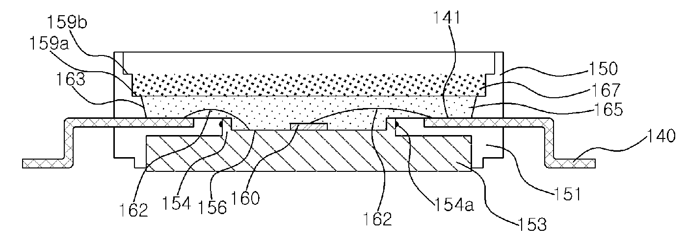
[0033]FIG. 2 is a sectional view illustrating a light emitting diode package 10 according to an embodiment of the present invention.

[0034]Referring to FIG. 2, the light emitting diode (LED) package 10 includes a pair of lead terminals 11 and 13 formed out of a lead frame, and a package main body 15. The main body 15 may be formed of a thermoplastic resin or a thermosetting resin using an insert molding process. In general, for the purpose of mass production of the LED package 10, a plurality of package main bodies 15 are formed in a lead panel where a plurality of lead frames are arranged. After molding resin (23, 25 or 27) has been cured, the lead frames are cut into individual LED packages 10, and the lead terminals 11 and 13 are consequently formed. The lead terminals 11 and 13 are disposed in such a manner that one ends thereof are close to face each ...


PUM


Abstract

Disclosed is a light emitting diode (LED) package having multiple molding resins. The LED package includes a pair of lead terminals. At least portions of the pair of lead terminals are embedded in a package main body. The package main body has an opening through which the pair of lead terminals is exposed. An LED die is mounted in the opening and electrically connected to the pair of lead terminals. A first molding resin covers the LED die. A second molding resin with higher hardness than the first molding resin covers the first molding resin. Therefore, stress to be imposed on the LED die can be reduced and the deformation of the molding resins can be prevented.

Description

TECHNICAL FIELD [0001]The present invention relates to a light emitting diode package having a molding resin, and more particularly, to a light emitting diode package, in which a light emitting diode die is covered with a molding resin having lower hardness and then with another molding resin having higher hardness in order to alleviate stress imposed on the light emitting diode die and to prevent the deformation of a top surface of the molding resin.BACKGROUND ART[0002]In general, a light emitting diode (LED) package includes a molding resin for covering a mounted LED die. The molding resin protects the LED die from the external environment. That is, the molding resin protects the LED die and the bonding wire from the external force and prevents the damage of the LED die by blocking moisture from the atmosphere. In addition, the molding resin may contain a phosphor that can change the wavelength of light emitted from the LED die. As the result, a white light can be obtained using a...

Claims


Application Information

Patent Timeline
IPC IPC(8): H01L29/22H01L33/50H01L33/54H01L33/56H01L33/62H01L33/64
CPCH01L33/52H01L33/56H01L33/62H01L33/642H01L33/647H01L2924/12041H01L2224/32245H01L2224/48247H01L2224/73265H01L2924/19107H01L33/486H01L2224/48091H01L2924/00014H01L2924/00012H01L2924/00
Inventor LEE, CHUNG-HOONKIM, DO-HYUNGLEE, KEON-YOUNG
Owner SEOUL SEMICONDUCTOR
Why Eureka
Try Eureka