Light emitting element, light emitting device having the same and method for manufacturing the same

a technology of light emitting elements and light emitting devices, which is applied in the direction of electrical devices, semiconductor devices, organic semiconductor devices, etc., can solve the problems of inability to apply inorganic compounds for capping layers, inflicting damage on the light emitting element itself, and being inferior in alignment accuracy of metal masks

Active Publication Date: 2008-01-31
LG DISPLAY CO LTD
View PDF11 Cites 64 Cited by
  • Summary
  • Abstract
  • Description
  • Claims
  • Application Information

AI Technical Summary

Benefits of technology

[0045] According to the first embodiment, a light emitting element comprises a capping layer which is provided on the outside of a transparent or semi-transparent electrode, with higher refractive index than the semi-transparent electrode. Therefore, the light emitting element can improve light extraction efficiency. Moreover, since the capping layer can be formed at temperature of 500° C. or lower by using compounds such as triarylamine derivative and / or carbazole derivative for the capping layer, the light extraction efficiency of each color can be optimized without the major damage to the light emitting element by using a mask with high accuracy. The light emitting element can be applied to full-color displays desirably, and a bright image with high color purity and high resolution can be displayed.
[0014] According to another aspect of the invention, a first method for manufacturing the first light emitting device in which the capping layers of the light emitting elements are made of a homogeneous material comprises depositing the material constituting the capping layer onto the second electrodes of the first and the second light emitting elements, to form a first layer onto the second electrodes of the first light emitting element, and to form the capping layer onto the second electrode of the second light emitting element, respectively. The first method also comprises depositing the material constituting the capping layer onto the first layer and onto the second electrode of the third light emitting element, respectively, to form the capping layer onto the second electrodes of the first and the third light emitting elements.

Problems solved by technology

It has been proposed that a metal mask with a high accuracy is used for forming a capping layer, however the metal mask has a problem of being inferior in alignment accuracy due to the deformation by heat.
Most of inorganic compounds are not suitable when using the mask having a high accuracy and also may inflict damage on the light emitting element itself, due to the high deposition temperature.
Moreover, since forming an inorganic layer by the sputter method may inflict damage on the light emitting element, the inorganic compounds are difficult to be applied for a capping layer.

Method used


Image

  • Light emitting element, light emitting device having the same and method for manufacturing the same
  • Light emitting element, light emitting device having the same and method for manufacturing the same
  • Light emitting element, light emitting device having the same and method for manufacturing the same

Examples


example

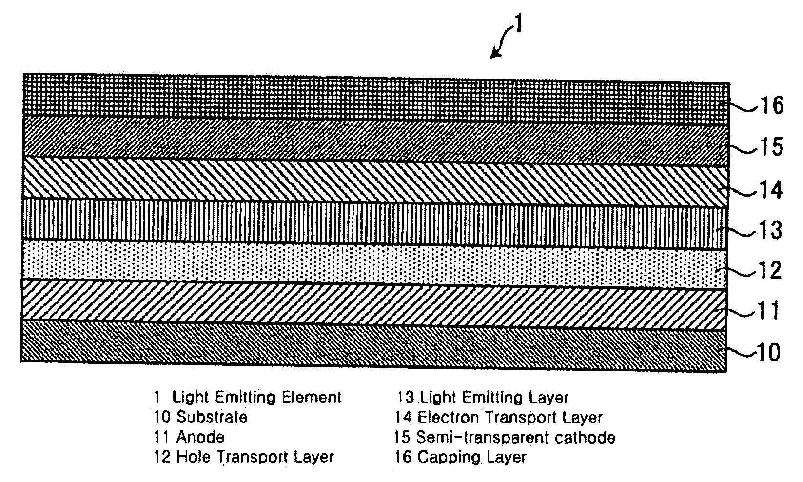
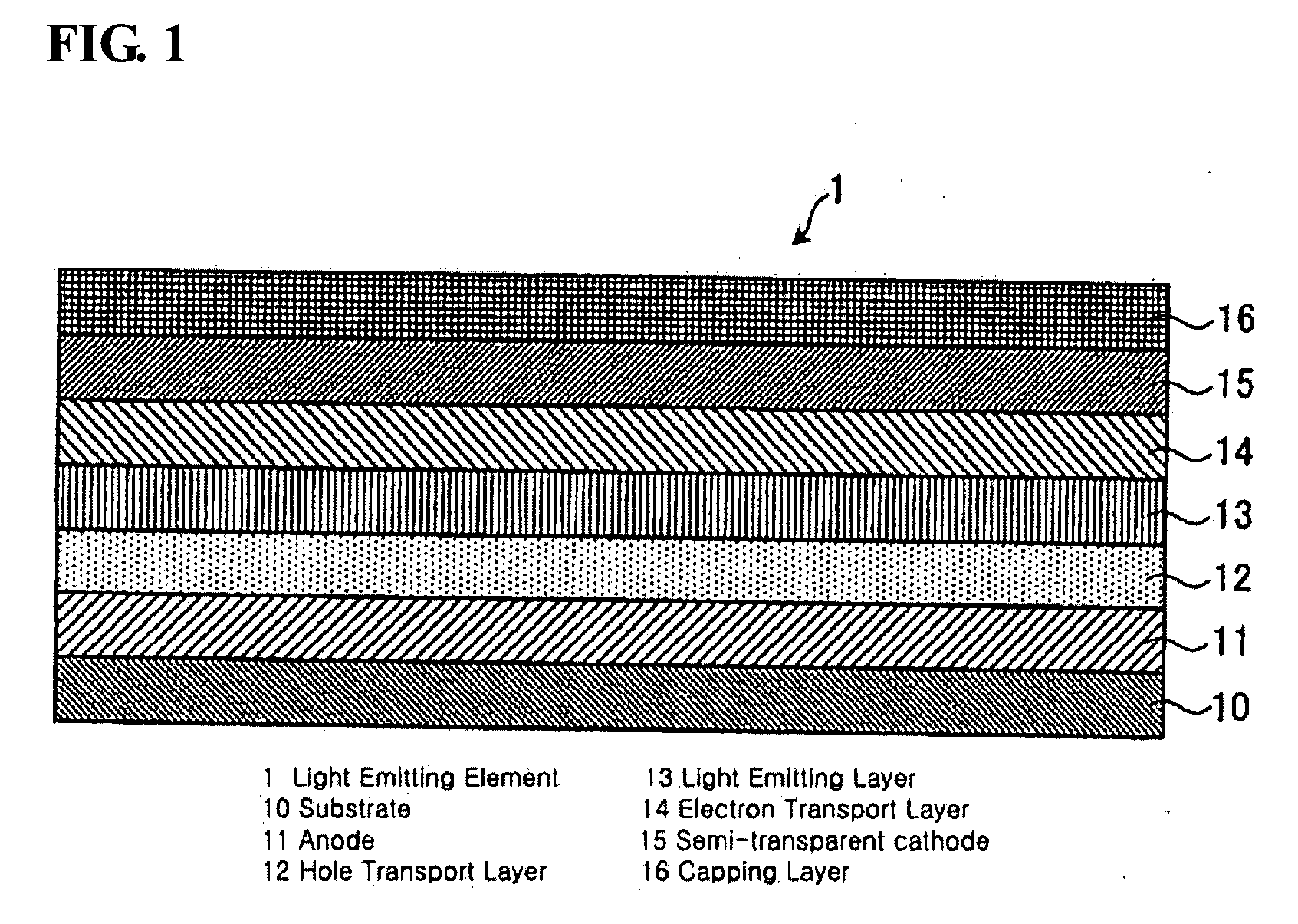
[0059] The example of the present invention will be explained more specifically. A red light emitting element of the present invention has been manufactured as below. First, Ni anode with layer thickness of 100 nm was laminated by sputtering method onto the substrate and then copper phthalocyanine (CuPc) with layer thickness of 20 nm as a hole injection layer was laminated through deposition method onto the Ni anode. Subsequently, N,N′-di(naphthalene-1-yl)-N,N′-diphenyl-benzidine (NPB) with layer thickness of 40 nm as a hole transport layer was laminated through deposition method. And then, Alq3 and 4-(dicyanomethylene)-2-t-butyl-6-(1,1,7,7,-tetramethyljulolidyl-9-enyl)-4H-pyran (DCJTB) as a light emitting layer were deposited by dual deposition. The layer thickness of Alq3 was 30 nm and 1% of DCJTB as the volume ratio was laminated simultaneously.

[0060] Then, Alq3 with layer thickness of 40 nm as an electron transport layer, and Ca with layer thickness of 12 nm and Mg with layer t...


PUM


Abstract

A light emitting element comprises a first electrode, a second electrode configured to transmitting light, an organic layer arranged between the first and the second electrodes, comprising a light emitting layer, and a capping layer arranged on the second electrode and made of a material with a higher refractive index than the refractive index of the material constituting the second electrode. The material constituting the capping layer comprises at least one selected from the group consisting of triarylamine derivative, carbazole derivative, benzimidazole derivative and triazole derivative.

Description

CROSS-REFERENCE TO RELATED APPLICATIONS [0001] The present application claims priority under 35 U.S.C. § 120 to PCT Application No. PCT / JP2006 / 305852, filed on Mar. 23, 2006, entitled “LUMINESCENT ELEMENT, LIGHT EMITTING DEVICE COMPRISING SAID LUMINESCENT ELEMENT, AND PROCESS FOR PRODUCING THE SAME”. The contents of this application are incorporated herein by reference in their entirety.BACKGROUND OF THE INVENTION [0002] 1. Field of the Invention [0003] The present invention relates to a light emitting element which is used in organic electroluminescent display devices, a light emitting device comprising the light emitting element, and a method for manufacturing the same. [0004] 2. Description of the Related Art [0005] An organic electroluminescent (EL) display device has properties such as thin type, wide viewing angle, low power consumption and excellent moving picture display and has been expected to be an image display device of the next generation. An organic electroluminescent...

Claims


Application Information

Patent Timeline
Patent Type & Authority Applications(United States)
IPC IPC(8): H01L33/00
CPCH01L27/3211H01L51/0059H01L51/0062H01L51/0065H01L2251/558H01L51/5237H01L51/5262H01L2251/5315H01L51/0081H10K59/35H10K85/649H10K85/631H10K85/653H10K85/324H10K50/844H10K50/85H10K2102/3026H10K2102/351H10K85/146H10K50/11H10K50/84H10K50/852
Inventor TAKEDA, KEIZOMURAKAMI, TOMOKO
Owner LG DISPLAY CO LTD
Why Eureka
Try Eureka