BORON DOPED SiGe HALO FOR NFET TO CONTROL SHORT CHANNEL EFFECT

a short channel effect and boron-doped sige technology, which is applied in the field of boron-doped sige halo for nfet to control can solve the problems of inability to adequately control the gate, the device typically cannot control the threshold voltage roll off, and the very short channel of the transistor, etc., to achieve better control of the short channel effect, low diffusion rate, and high solid solubility of boron

Inactive Publication Date: 2008-01-31
IBM CORP +1
View PDF9 Cites 30 Cited by
  • Summary
  • Abstract
  • Description
  • Claims
  • Application Information

AI Technical Summary

Benefits of technology

[0006]An n-type field effect transistor (NFET) and methods of forming a halo for an NFET to control the short channel effect (SCE) are disclosed. One method includes forming a gate over a silicon substrate; recessing the silicon adjacent to the gate; forming a halo by epitaxially growing boron in-situ doped silicon germanium (SiGe) in the recess; and epitaxially growing un-doped silicon over the silicon germanium. Alternatively, the halo can be formed by ion implanting boron into an embedded SiGe region within the

Problems solved by technology

As a result, transistors with very short channels suffer from problems related to the inability of the gate to adequately control the “on” and “off” states of the channel.
For example, these devices typically cannot control threshold voltage

Method used


Image

  • BORON DOPED SiGe HALO FOR NFET TO CONTROL SHORT CHANNEL EFFECT
  • BORON DOPED SiGe HALO FOR NFET TO CONTROL SHORT CHANNEL EFFECT
  • BORON DOPED SiGe HALO FOR NFET TO CONTROL SHORT CHANNEL EFFECT

Examples


Embodiment Construction

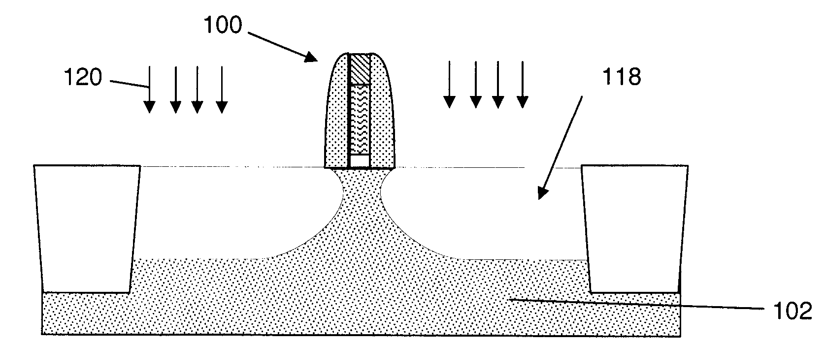
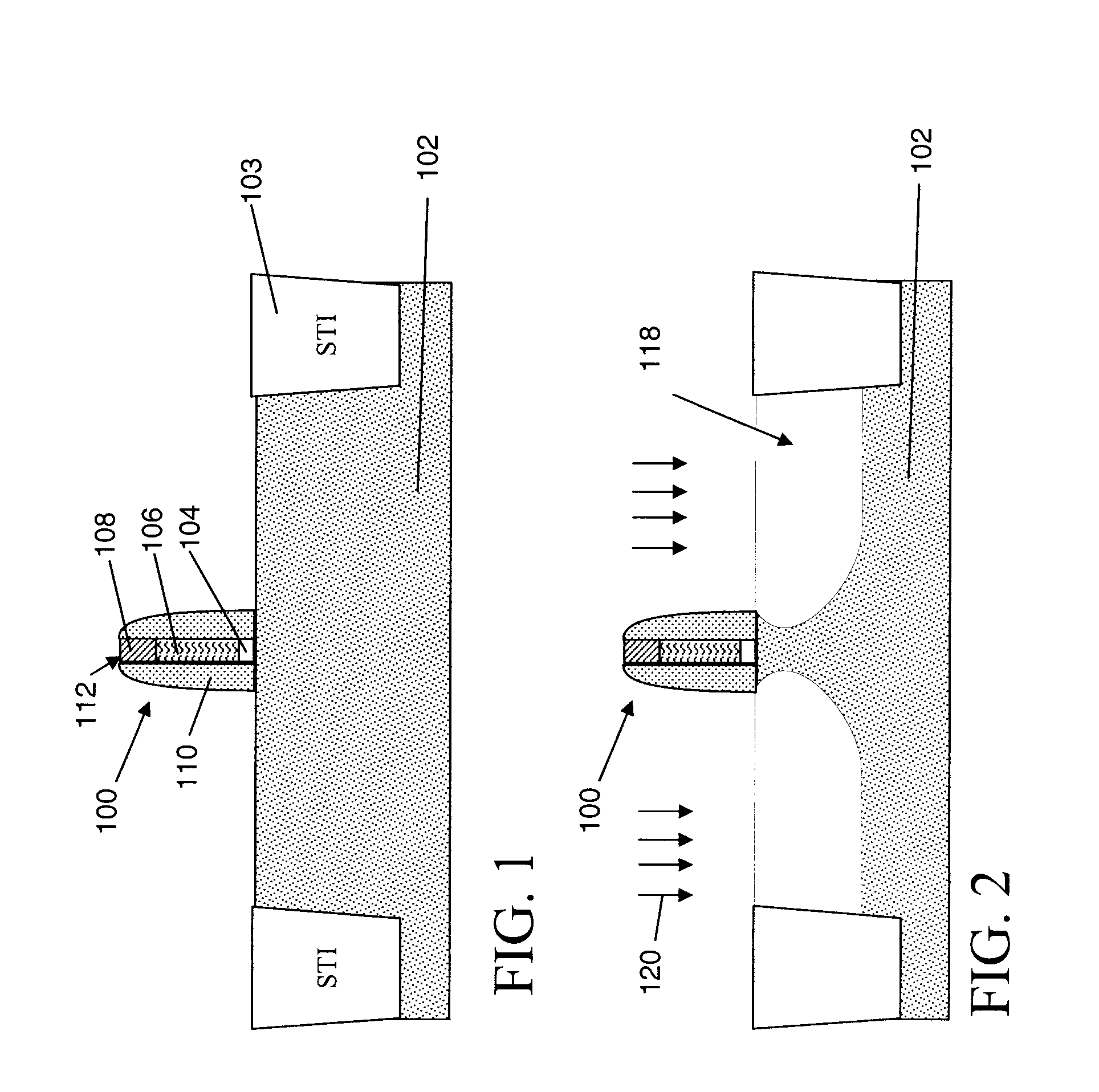
[0015]Turning to the drawings, embodiments of a method of forming a halo for an n-type field effect transistor (NFET) will now be described. In FIG. 1, a gate 100 is formed over a silicon substrate 102. Shallow trench isolations (STI) 103 may be formed in silicon substrate 102 in a conventional manner. Silicon substrate 102 may include a bulk silicon (shown) or be provided as a silicon-on-insulator (SOI) substrate. Gate 100 may be formed using any now known or later developed technique such as depositing or growing a gate dielectric 104, depositing polysilicon 106, forming a silicon nitride (Si3N4) cap 108, and then forming, patterning and etching (e.g., reaction ion etching (RIE)) to form gate stack 112. A spacer 110 may be formed about gate stack 112 to arrive at gate 100. Although not shown, source / drain extensions may be implanted at this stage. In any event, gate 100 may ultimately have an ultra-short channel length, e.g., well below the 100 nm regime, thus making it susceptibl...


PUM


Abstract

An n-type field effect transistor (NFET) and methods of forming a halo for an NFET to control the short channel effect are disclosed. One method includes forming a gate over a silicon substrate; recessing the silicon adjacent to the gate; forming a halo by epitaxially growing boron in-situ doped silicon germanium (SiGe) in the recess; and epitaxially growing silicon over the silicon germanium. Alternatively, the halo can be formed by ion implanting boron into an embedded SiGe region within the silicon substrate. The resulting NFET includes a boron doped SiGe halo embedded within the silicon substrate. The embedded SiGe layer may be a relaxed layer without inserting strain in the channel. The high solid solubility of boron in SiGe and low diffusion rate allows formation of a halo that will maintain the sharp profile, which provides better control of the short channel effect and increasing control over NFET threshold voltage roll-off.

Description

BACKGROUND OF THE INVENTION[0001]1. Technical Field[0002]The invention relates generally to semiconductor device fabrication, and more particularly, to an n-type field effect transistor (NFET) and methods of forming a halo for an NFET to control the short channel effect.[0003]2. Background Art[0004]The continual reduction in the size of metal-oxide semiconductor (MOS) devices has provided significant improvement in circuit density and device performance. As the device channel length of conventional planar MOS field effect transistors (MOSFETs) continues to decrease, the interaction between the source / drain (S / D) and the channel increases, and the S / D begins to gain influence on the channel potential. As a result, transistors with very short channels suffer from problems related to the inability of the gate to adequately control the “on” and “off” states of the channel. For example, these devices typically cannot control threshold voltage roll off. This situation is referred to as th...

Claims


Application Information

Patent Timeline
IPC IPC(8): H01L29/76H01L21/336
CPCH01L21/26586H01L29/1045H01L29/165H01L29/66636H01L29/6656H01L29/66628H01L29/665
Inventor CHEN, XIANGDONGCHONG, YUNG FULUO, ZHIJIONGWANG, XINLINYANG, HAINING S.
Owner IBM CORP
Why Eureka
Try Eureka