Method for treating parasitic resistance, capacitance, and inductance in the design flow of integrated circuit extraction, simulations, and analyses

a semiconductor device and design flow technology, applied in the field of methods for calculating parasitic resistance, capacitance and inductance in the design flow of integrated circuits, can solve problems such as unanticipated and unwanted delays, functional failures, and inability to accurately model or calcula

Inactive Publication Date: 2008-01-31
IBM CORP
View PDF17 Cites 53 Cited by
  • Summary
  • Abstract
  • Description
  • Claims
  • Application Information

AI Technical Summary

Benefits of technology

[0012]Bearing in mind the problems and deficiencies of the prior art, it is therefore an object of the present invention to provide a method of addressing parasitic resistance, inductance, and capacitance in an extraction tool that is not limited to the best case, worst case, and nominal values only.

Problems solved by technology

For instance, signal line parasitic capacitance has a detrimental role in signal propagation, causing unanticipated and unwanted delays.
Interconnect parasitics have at least two effects: 1) delay due to different switching patterns; and 2) induced glitches or noise that could cause functional failure by switching logic states.
Unlike the signal delay in an active device itself, which is usually well characterized and within an analytical tool's device library, a line delay depends on the structures in the vicinity of the line, and thus cannot be accurately modeled or calculated until all the circuit elements associated with the signal path are placed and routed.
Thus, signal propagation delay due to parasitic-induced coupling is difficult to predict and accommodate through design enhancements without an accurate estimate of its overall effect in the circuit layout.
The exact closed-form method is limited in geometry, and not practical for application with highly dense integrated circuit topologies.
Approximate formulae are generally used in extraction programs, but lack the accuracy necessary to predict capacitance and inductance coupling for advanced integrated circuit chips.
Unfortunately, the number of nodes that need to be entered in a VLSI chip is quite large, and could be overwhelming.
Models used to extract and estimate parasitic resistance, capacitance, and inductance values have been employed in the prior art with success, but with considerable design limitations.
In the prior art methodologies described above, and in many others generally used in the industry, device models employed do not account for the parasitic couplings from interconnect wires.
The prior art lacks the capability to include variations of parasitic resistance, capacitance, and inductance for analysis.
The prior art is further deficient in considering the variations of parasitics on worst case circuit performance.
Moreover, under the current analytical regimes, due to the discrete nature of the data, worst case or best case circuit performance may not be relied upon to be sufficiently accurate.

Method used


Image

  • Method for treating parasitic resistance, capacitance, and inductance in the design flow of integrated circuit extraction, simulations, and analyses
  • Method for treating parasitic resistance, capacitance, and inductance in the design flow of integrated circuit extraction, simulations, and analyses
  • Method for treating parasitic resistance, capacitance, and inductance in the design flow of integrated circuit extraction, simulations, and analyses

Examples


Embodiment Construction

)

[0029]In describing the preferred embodiment of the present invention, reference will be made herein to FIGS. 1-9 of the drawings in which like numerals refer to like features of the invention.

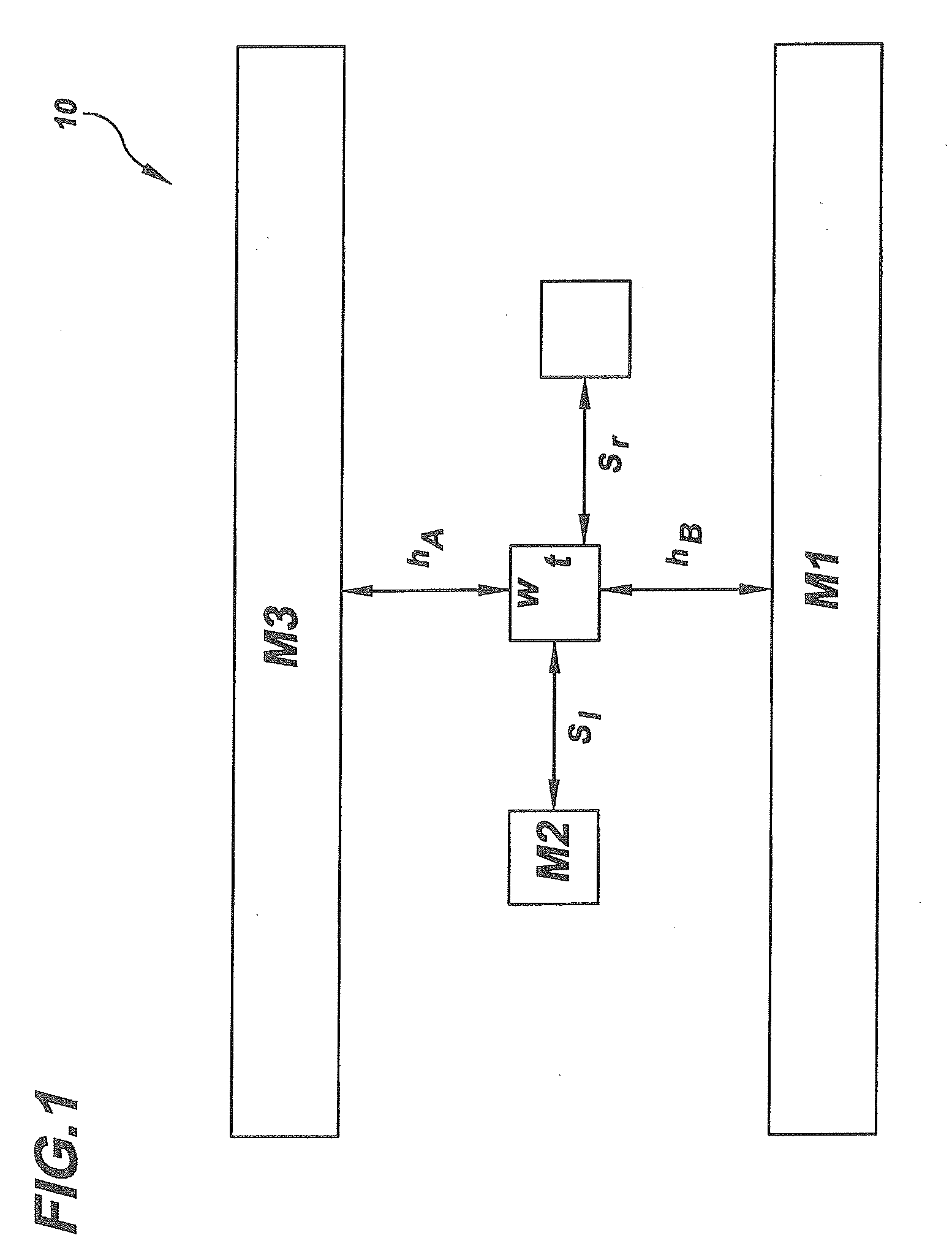
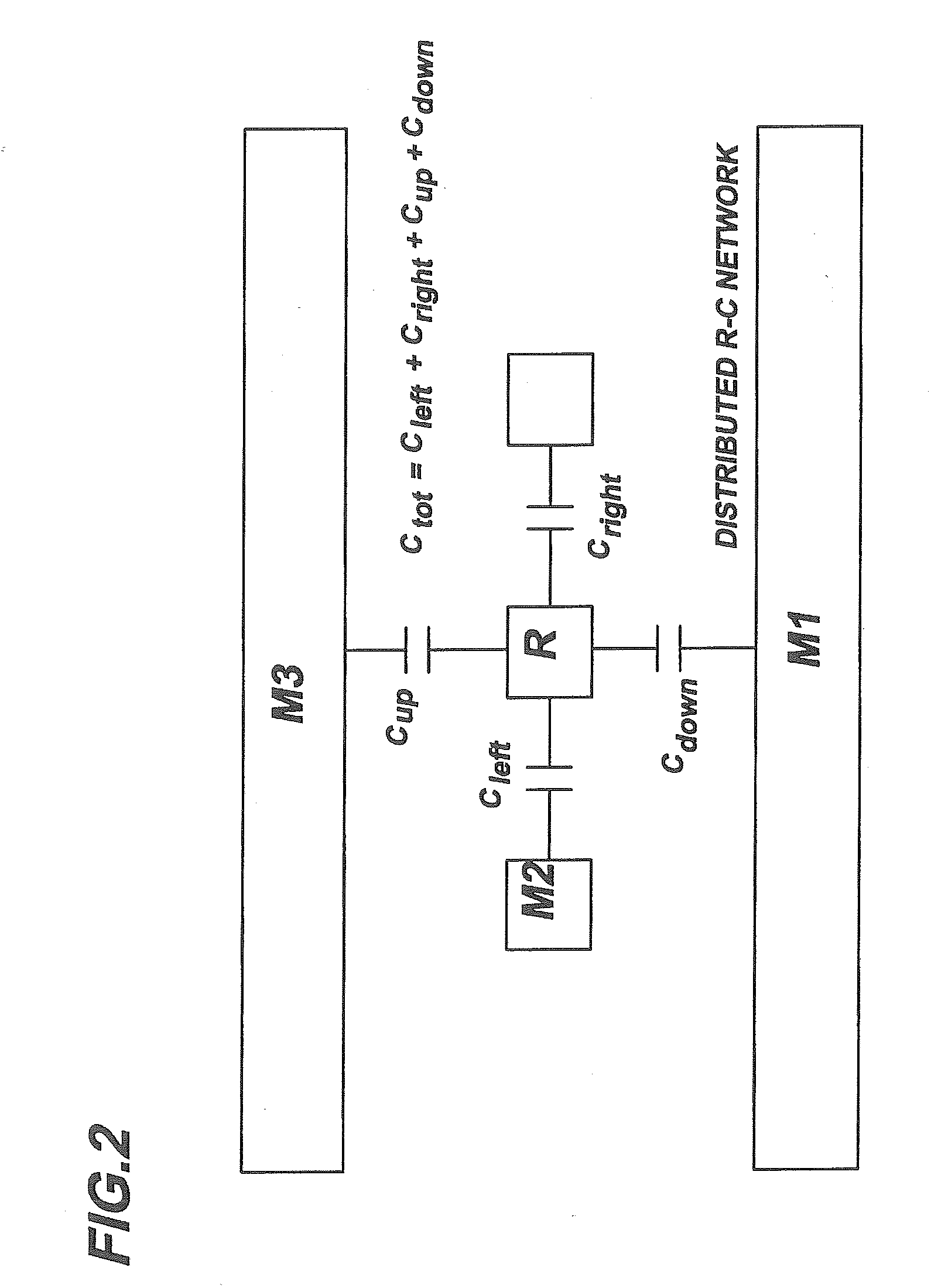
[0030]FIG. 1 depicts a two-dimensional model 10 of the present invention simulating wire parasitic capacitance and resistance. Two current carrying, parallel metal signal or interconnect lines M1 and M3 are shown a distance hA and hB, respectively, from three interconnect lines M2, which are perpendicular to the direction and layout of M1 and M3 (shown in the figure as going through the page). The interconnect lines have a known width w and height or thickness t, and are placed a distance s1 from the (first) neighboring wire on the left, and a distance sr from the (first) neighboring wire on the right. The resistance of M2 is at a minimum when the width w and thickness t are maximized. Under this condition, the line-to-line coupling capacitance, CM2-M2 (including both Cleft, and Cright), the ...


PUM


Abstract

An extraction, simulation, and analysis combined method is employed to account for the parasitic couplings from interconnect wires. Variations of parasitic resistance, capacitance, and inductance are used in circuit analysis calculators, including considering the variations of the parasitics on worst case circuit performance, skewing, and statistical Monte Carlo analysis. Each parasitic element is modeled as a call-up function with associated process distributions. Circuit analysis, such as a SPICE analysis is performed on the selected models.

Description

BACKGROUND OF THE INVENTION[0001]1. Field of the Invention[0002]This invention relates to a method for calculating parasitic resistance, capacitance, and inductance in a semiconductor device design. More particularly, the invention relates to Very Large Scale Integrated Circuit (VLSI) chips utilizing submicron technology, and specifically to a method of calculating and treating parasitic resistance, capacitance, and inductance in the design flow of integrated circuit extraction, simulations, and analyses.[0003]2. Description of Related Art[0004]Large interconnect parasitic resistances, capacitances, and inductances play an important role in assessing the delay of signals and in predicting the effects of system-generated noise. The parasitic information, once extracted, may be used in chip timing calculations and noise induction. In VLSI designs, on-chip signal delay is increasingly dominated by the RC delay associated with signal lines. The dielectric structures available in advance...

Claims


Application Information

Patent Timeline
Patent Type & Authority Applications(United States)
IPC IPC(8): G06F17/50
CPCG06F17/5036G06F30/367
Inventor LU, NINGSPRINGER, SCOTT K.
Owner IBM CORP
Why Eureka
Try Eureka