Trenched MOSFET device with trenched contacts

Active Publication Date: 2008-02-14
FORCE MOS TECH CO LTD
View PDF3 Cites 27 Cited by
  • Summary
  • Abstract
  • Description
  • Claims
  • Application Information

AI Technical Summary

Benefits of technology

[0009]It is therefore an object of the present invention to provide new and improved semiconductor power device configuration, such as a MOSFET device that comprises tungsten contact plugs disposed in trenches disposed away from the trench intersection areas. By opening contact trenches away from the trench intersection areas and away from the trench center, the problem of etching through polysilicon holes due to the etching process in opening the trenches for contact plugs is minimized. The problems as that encountered in the manufacturing processes as discussed above are resolved.
[0010]Briefly, in a preferred embodiment, the present invention discloses a trenched semiconductor power device that includes a trenched gate disposed in an extended continuous trench surrounding a plurality of transistor cells in an active cell area and extending as trench-gate fingers to intersect with a trenched gate under the gate metal runner at a termination area. At least one of the trench-gate fingers intersects with the trenched gate under the gate metal runner near the termination area having trench intersection regions vulnerable to have a polysilicon void developed therein. At least a gate contact trench opened through an insulation layer covering the semiconductor power device wherein the gate contact trench penetrating from the insulation layer and extending into the gate polysilicon and the gate contact trench is opened in an area away from the trench intersection regions where the polysilicon voids may be formed, and away from a center portion of the trench gate under the gate metal runner where a polysilicon seam is formed. In a preferred embodiment, the trench intersection regions constitute a T-shaped intersection region. In a preferred embodiment, the gate contact trench is filled with a conductive gate contact plug. In a preferred embodiment, the gate contact trench is filled with a tungsten gate contact plug. In a preferred embodiment, the gate contact trench is filled with a tungsten gate contact plug surrounded with a Ti/TiN barrier layer. In a preferred embodiment, the gate contact trench is filled with a Ti/TiN/Al alloys. In a preferred embodiment, the trenched gate under the gate metal runner is configured as an open stripe extending from and intersecting to the trench-gate fingers as an L-shaped trenched gate under the gate metal runner with the width of gate contact trench smaller than hal

Problems solved by technology

However, with tungsten plugs implemented as source and gate contact, there are still additional technical challenges confronted with such device configuration and manufacturing processes.
Potential problems may arise in carrying out the contact silicon etch due to the possibility of etching through the polysilicon gate unless special layout are prearranged to preve

Method used


Image

  • Trenched MOSFET device with trenched contacts
  • Trenched MOSFET device with trenched contacts
  • Trenched MOSFET device with trenched contacts

Examples


Example

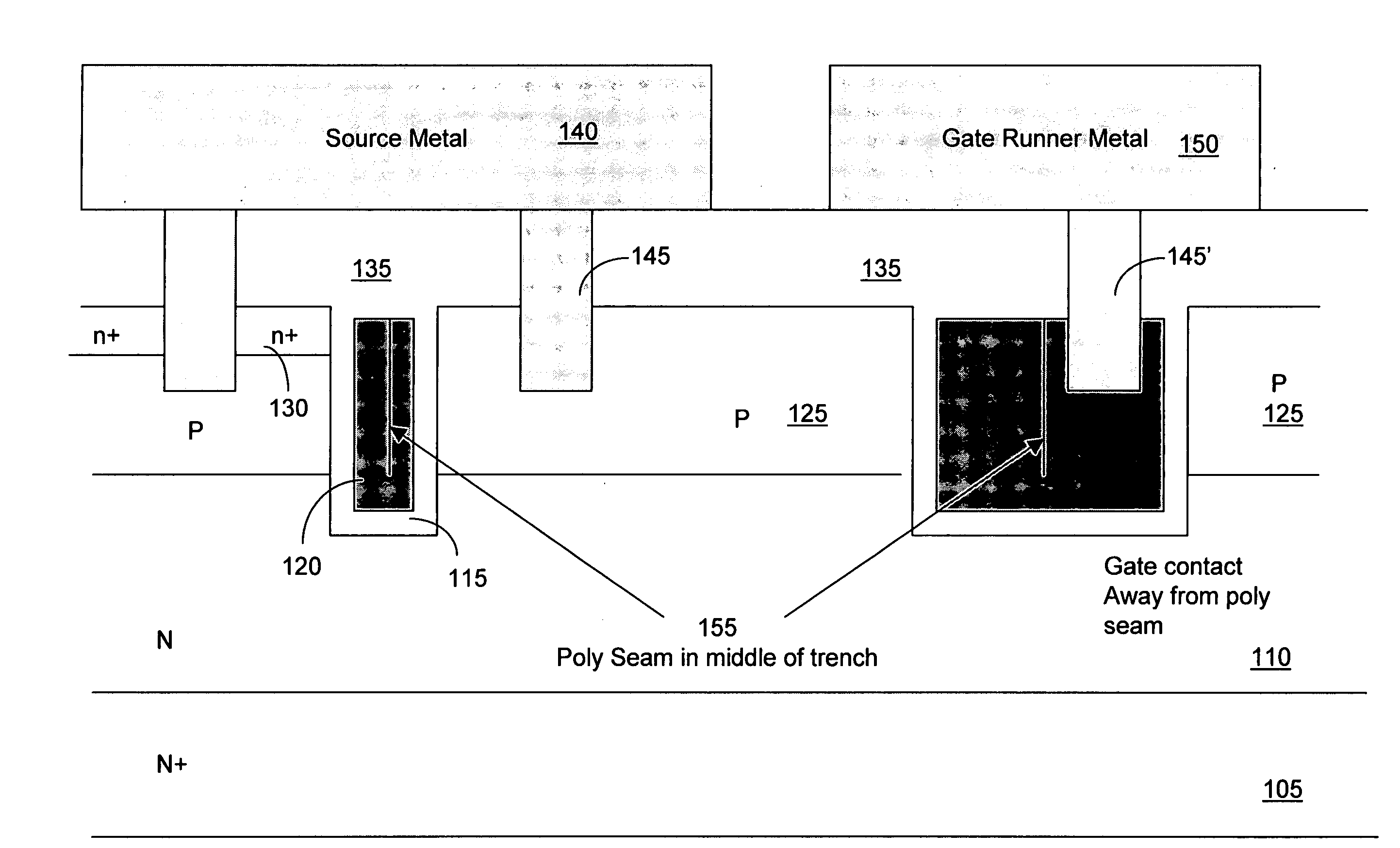
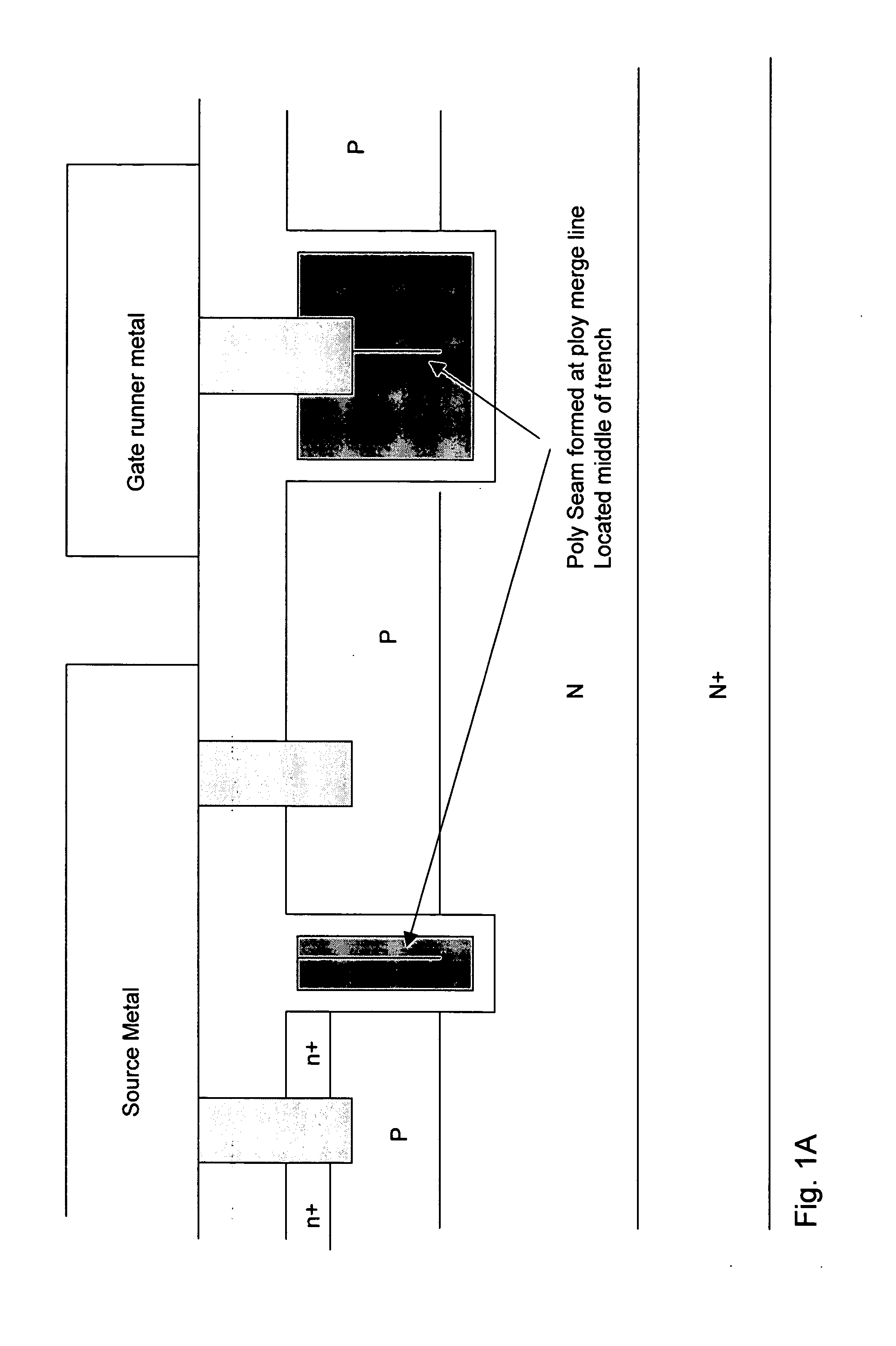
[0016]Please refer to FIGS. 2A to 2C for the side cross sectional view and two top views of a first preferred embodiment of this invention. A metal oxide semiconductor field effect transistor (MOSFET) device 100 is supported on a substrate 105 formed with an epitaxial layer 110. The MOSFET device 100 includes a trenched gate 120 disposed in a trench with a gate insulation layer 115 formed over the walls of the trench. A body region 125 that is doped with a dopant of second conductivity type, e.g., P-type dopant, extends between the trenched gates 120. The P-body regions 125 encompassing a source region 130 doped with the dopant of first conductivity, e.g., N+ dopant. The source regions 130 are formed near the top surface of the epitaxial layer surrounding the trenched gates 120. The top surface of the semiconductor substrate extending over the top of the trenched gate, the P body regions 125 and the source regions 130 are covered with a NSG and a BPSG dielectric layers 135. A source...


PUM


Abstract

A trenched semiconductor power device that includes a trenched gate disposed in an extended continuous trench surrounding a plurality of transistor cells in an active cell area and extending as trench-gate fingers to intersect with a trenched gate under the gate metal runner at a termination area. At least one of the trench-gate fingers intersects with the trenched gate under the gate metal runner near the termination area having trench intersection regions vulnerable to have a polysilicon void and seam developed therein. At least a gate contact trench opened through an insulation layer covering the semiconductor power device wherein the gate contact trench penetrating from the insulation layer and extending into the gate polysilicon and the gate contact trench is opened in an area away from the trench intersection regions and also away from a center portion of said the trenched gate underneath said gate runner metal where a polysilicon void or a seam is likely formed thus avoid the formation of the vulnerable spots.

Description

BACKGROUND OF THE INVENTION[0001]This Formal Application claims a Priority Date of Aug. 8, 2006 benefited from a Provisional Patent Applications 60 / 836,344 filed by the same Applicant of this Application.[0002]1. Field of the Invention[0003]This invention relates generally to the cell structure, device configuration and fabrication process of power semiconductor devices. More particularly, this invention relates to a novel and improved cell structure, device configuration and improved process for fabricating a trenched semiconductor power device with improved increased cell density by reducing a gate to source contact critical dimension (CD) requirement.[0004]2. Description of the Related Art[0005]In order to further increase the cell density in a semiconductor power device, the MOSFET devices are manufactured with trenched source contact plugs with the plugs formed with tungsten to reduce the distance between the gate and the source contact. Specifically, the Applicant of this Pate...

Claims


Application Information

Patent Timeline
IPC IPC(8): H01L29/94H01L29/76H01L31/00
CPCH01L29/402H01L29/41766H01L29/4236H01L29/42372H01L29/7813H01L29/4238H01L29/456H01L29/4941H01L29/7811H01L29/42376
Inventor HSHIEH, FWU-IUAN
Owner FORCE MOS TECH CO LTD
Why Eureka
Try Eureka