
Semiconductor device and method for manufacturing the same

Inactive Publication Date: 2008-02-14
PANASONIC CORP
View PDF8 Cites 23 Cited by
  • Summary
  • Abstract
  • Description
  • Claims
  • Application Information

AI Technical Summary

Benefits of technology

[0012]In the conventional example shown in FIG. 14A to FIG. 14D, however, the high dielectric insulating film 105 is used as both the gate insulating film of the MIS transistor as the low voltage using element formed in the core region and the gate insulating film of the MIS transistor as the high voltage using element formed in the I / O region, and therefore, the semiconductor device cannot cope with such the cases. In other words, the reliability of the gate insulating film of the MIS transistor formed in the I / O region is lowered.
[0014]For coping with the foregoing, Patent Document 1 provides a technique of separate formation of gate insulating films having different dielectric constants between the MIS transistor of the high voltage using element and the MIS transistor of the low voltage using element. This technique, however, requires separate formation of gate electrodes and of sidewall spacers for the MIS transistors in the respective voltage using elements, thereby complicating the manufacturing method.
[0015]In view of the foregoing, the present invention has its object of providing a structure of a semiconductor device in which plural kinds of gate insulating films having different dielectric constants are used separately on a single substrate according to necessity and a simple method for attaining the structure.
[0046]According to the present invention, a structure of a semiconductor device in which plural kinds of gate insulating films having different dielectric constants are used in a single substrate separately according to necessity can be attained by a simple manufacturing method. Hence, high-level enhancement of both the chip performance and the reliability can be achieved.
[0047]In sum, the present invention relates to a semiconductor device on which MIS transistors including gate insulating films having various film thicknesses are boarded and manufacturing method thereof, can achieve high-level enhancement of both the chip performance and the reliability when the present invention is applied to various kinds of electronic equipment, and is therefore very useful.

Problems solved by technology

While, such a high dielectric gate insulating film is not necessarily needed for a high voltage using element and is undesirable in some cases because the reliability of the high dielectric gate insulating film is lowered by high voltage application.
In the conventional example shown in FIG. 14A to FIG. 14D, however, the high dielectric insulating film 105 is used as both the gate insulating film of the MIS transistor as the low voltage using element formed in the core region and the gate insulating film of the MIS transistor as the high voltage using element formed in the I / O region, and therefore, the semiconductor device cannot cope with such the cases.
This technique, however, requires separate formation of gate electrodes and of sidewall spacers for the MIS transistors in the respective voltage using elements, thereby complicating the manufacturing method.

Method used


Image

  • Semiconductor device and method for manufacturing the same
  • Semiconductor device and method for manufacturing the same
  • Semiconductor device and method for manufacturing the same

Examples


embodiment 1

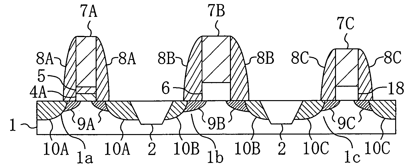
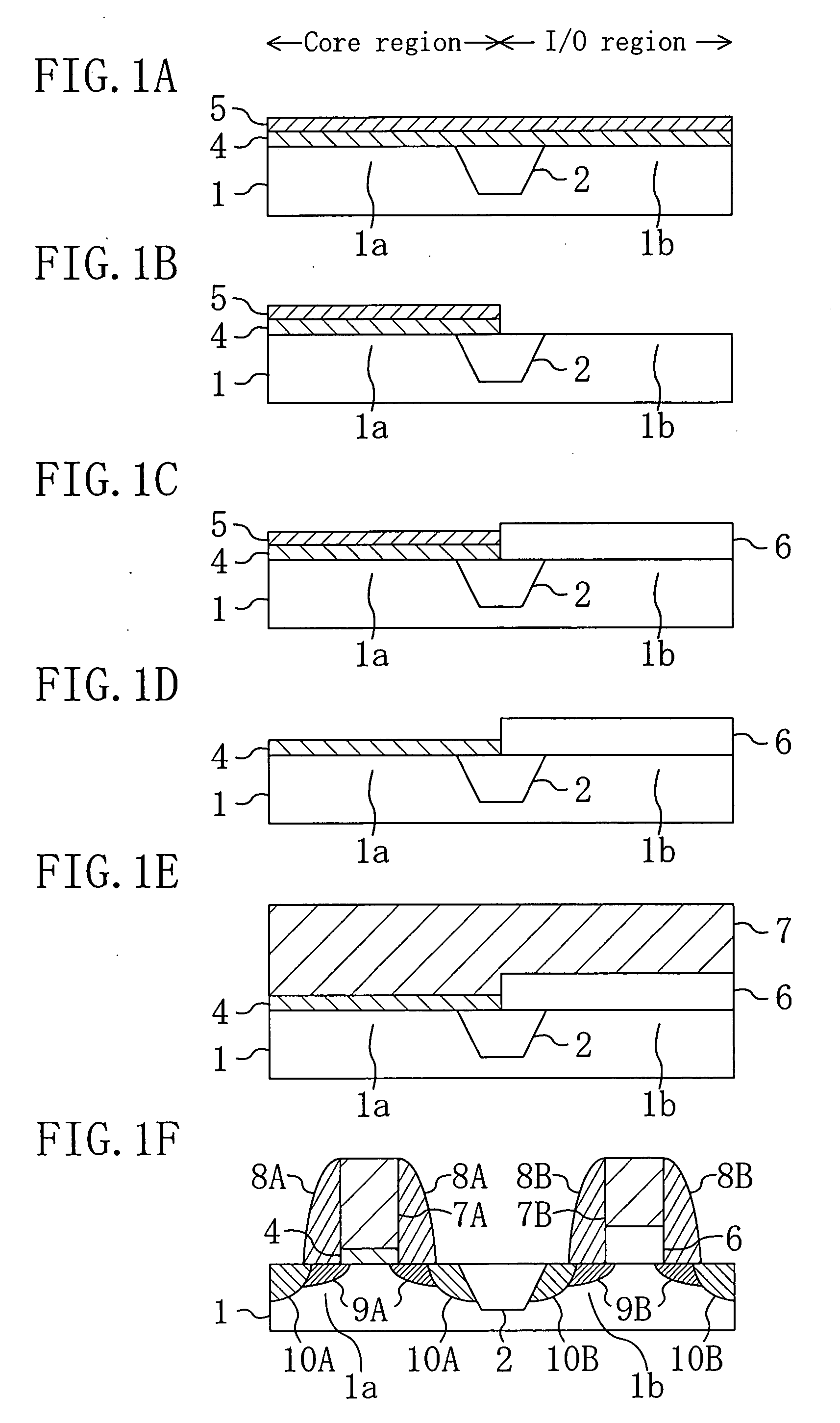
[0062]A semiconductor device and a manufacturing method thereof in accordance with Embodiment 1 of the present invention will be described below with reference to the drawings by referring to an example where the structure in the present embodiment is applied to N-type MIS transistors.

[0063]FIG. 1A to FIG. 1F are sectional view showing respective steps of the semiconductor device manufacturing method in accordance with the present embodiment. In the present embodiment, a core region means a region where an N-type MIS transistor composing a logic circuit or the like using relatively low voltage is formed, and an I / O region means a region where an N-type MIS transistor composing an I / O circuit or the like using relatively high voltage is formed.

[0064]First, as shown in FIG. 1A, an isolation region 2 of, for example, a STI is formed in a one conductivity type substrate (semiconductor substrate) including a semiconductor region, such as a silicon region or the like to define the core re...

modified example of embodiment 1

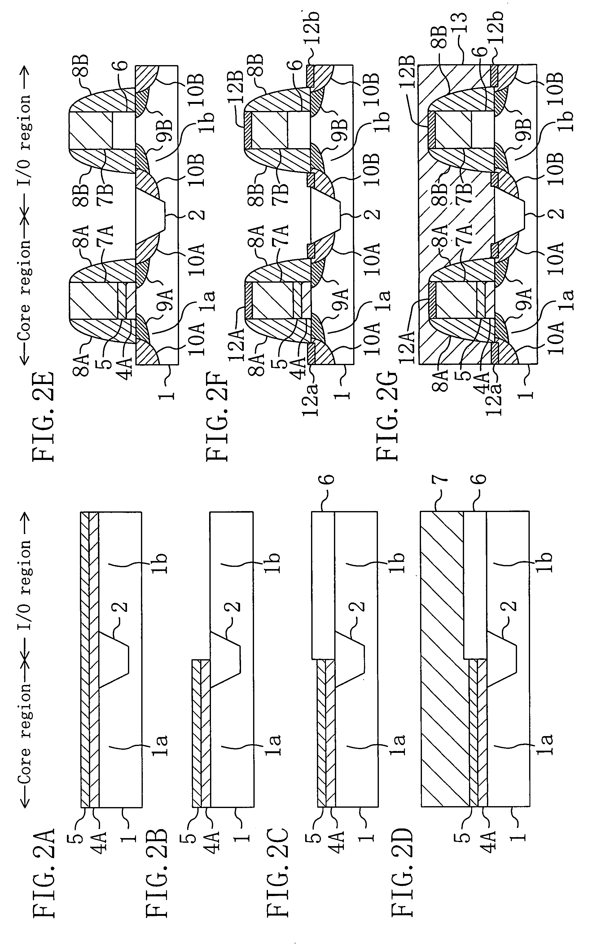
[0083]A semiconductor device and a manufacturing method thereof in accordance with a modified example of Embodiment 1 of the present invention will be described with reference to the drawings by refereeing to an example where the structure in the present modified example is applied to N-type MIS transistors.

[0084]FIG. 2A to FIG. 2G are sectional views showing respective steps of the semiconductor device manufacturing method in accordance with the present modified example. In FIG. 2A to FIG. 2G, the same reference numerals are assigned to the same elements as those in Embodiment 1 shown in FIG. 1A to FIG. 1F for omitting duplicate description. Further, in the present modified example, the core region means a region where an N-type MIS transistor composing a logic circuit or the like using relatively low voltage is formed, and the I / O region means a region where an N-type MIS transistor composing an I / O circuit or the like using relatively high voltage is formed.

[0085]Significant diff...

embodiment 2

[0103]A semiconductor device and a manufacturing method thereof in accordance with Embodiment 2 of the present invention will be described below with reference to the drawings.

[0104]FIG. 3A is a sectional view of the semiconductor device in the gate length direction in accordance with the present embodiment, and FIG. 3B is a sectional view with a partially enlarged view of the semiconductor device in the gate width direction in accordance with the present embodiment. In FIG. 3A and FIG. 3B, the same reference numerals are assigned to the same elements as those in Embodiment 1 shown in FIG. 1A to FIG. 1F or in the modified example thereof shown in FIG. 2A to FIG. 2G for omitting duplicate description. In the present embodiment, an N-channel region means a region where an N-type MIS transistor is formed, and a P-channel region means a region where a P-type MIS transistor is formed.

[0105]Referring to the modified example of Embodiment 1 shown in FIG. 2A to FIG. 2G, the layered structur...


PUM


Abstract

A semiconductor device includes a first MIS transistor and a second MIS transistor. The first MIS transistor includes: a first gate insulating film formed on a first active region of a substrate; and a first gate electrode formed on the first gate insulating film. The second MIS transistor includes: a second gate insulating film formed on a second active region of the substrate and having a dielectric constant lower than the first gate insulating film; and a second gate electrode formed on the second gate insulating film. Insulting sidewall spacers having the same structure are formed on respective side faces of the first gate electrode and the second gate electrode.

Description

BACKGROUND OF THE INVENTION[0001]1. Field of the Invention[0002]The present invention relates to structures of semiconductor devices and manufacturing methods thereof, and particularly relates to a semiconductor device on which MISFETs (Metal Insulator Semiconductor Field Effect Transistors) including gate insulating films having various thickness are boarded and a manufacturing method thereof.[0003]2. Related Art[0004]Recent progress in high integration, enhanced functions, and high-speed operation of semiconductor integrated circuits brings promotion of scaling of gate insulating films of MISFETs (hereinafter referred to it as a MIS transistor). When the gate insulating film is reduced in film thickness to some extent, leak current caused due to direct tunneling increases dramatically, so that power consumption of chips cannot be ignored, which means that an oxide film as a conventional gate insulating film almost reaches the limit in thickness reduction. In view of this, the atte...

Claims


Application Information

Patent Timeline
IPC IPC(8): H01L29/78H01L21/8238
CPCH01L21/82345H01L21/823462H01L21/823468H01L21/823878H01L21/823842H01L21/823857H01L21/823864H01L21/823481
Inventor HIRASE, JUNJISATO, YOSHIHIRO
Owner PANASONIC CORP
Features
  • Generate Ideas
  • Intellectual Property
  • Life Sciences
  • Materials
  • Tech Scout
  • Unparalleled Data Quality
  • Higher Quality Content
  • 60% Fewer Hallucinations
Learn More