Active-matrix-type light-emitting device, electronic apparatus, and pixel driving method for active-matrix-type light-emitting device

a technology of active matrix and light-emitting device, which is applied in the direction of static indicating device, electroluminescent light source, instruments, etc., can solve the problems of limited display pixels, limited lifetime and power consumption, and problem of optical leakage current of tft, so as to effectively suppress the increase in black level and reduce the effect of coupling curren

Active Publication Date: 2008-02-14
ELEMENT CAPITAL COMMERCIAL CO PTE LTD
View PDF14 Cites 127 Cited by
  • Summary
  • Abstract
  • Description
  • Claims
  • Application Information

AI Technical Summary

Benefits of technology

[0046]In the pixel driving method according to the aspect of the invention, the coupling current can be reduced by decreasing the

Problems solved by technology

In the case of the passive matrix driving method, the number of display pixels is limited and there are limitations in terms of lifetime and power consumption.
In JP-A-2006-17966, the optical leak current of the TFT is an issue.
However, the leak current generated in the TFT also includes a leak current (dark current) generated when the TFT is in an OFF state and a leak current generated due to a circuit operation.
As a result, since a black level rises, the contrast decreases, thus sin

Method used


Image

  • Active-matrix-type light-emitting device, electronic apparatus, and pixel driving method for active-matrix-type light-emitting device
  • Active-matrix-type light-emitting device, electronic apparatus, and pixel driving method for active-matrix-type light-emitting device
  • Active-matrix-type light-emitting device, electronic apparatus, and pixel driving method for active-matrix-type light-emitting device

Examples


first embodiment

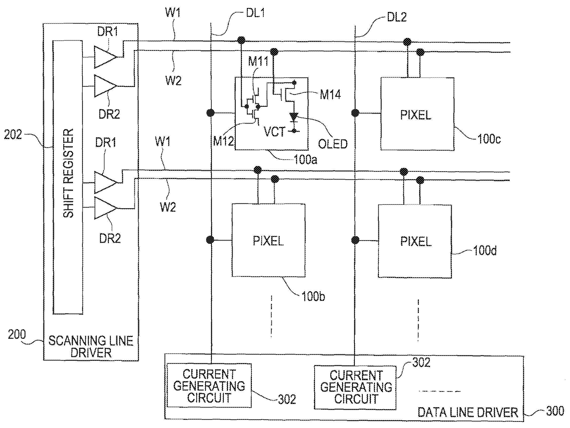
[0081]FIG. 1 is a circuit diagram illustrating the overall configuration of an example (organic EL panel based on a current programming method) of an active-matrix-type light-emitting device according to an embodiment of the invention.

[0082]As shown in the drawing, the active-matrix-type light-emitting device of FIG. 1 includes active-matrix-type pixels (pixel circuits) 100a to 100d, a scanning line driver (scanning line driving circuit) 200, a data line driver (data line driving circuit) 300, first and second scanning lines W1 and W2, and data lines DL1 and DL2.

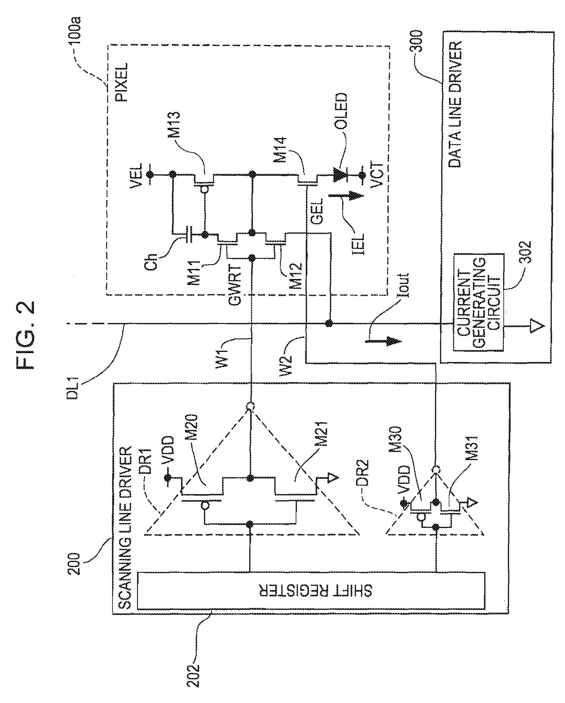
[0083]Each of the pixels (pixel circuits) 103a to 100d includes NMOSTFTs M11 and M12, which are driven through the first scanning sine W1 and serve as control transistors, an emission control transistor M14 driven through the second scanning line W2, and an organic EL element OLED.

[0084]In addition, the scanning line driver 200 includes a shift register 202, an output buffer DR1 for driving the first scanning line W1, and an...

second embodiment

[0113]FIG. 6 is a circuit diagram illustrating the circuit configuration of an example (example in which the current drive capability is reduced by connecting a current restricting resistor to an output end of an output buffer that drives a second scanning line) of an active-matrix-type light-emitting device according to another embodiment of the invention. In FIG. 6, the same components as in FIG. 2 are denoted by the same reference numerals.

[0114]The circuit configuration of the active-matrix-type light-emitting device shown in FIG. 6 is almost the same as the circuit configuration of the circuit shown in FIG. 2. However, in FIG. 6, the sizes (channel conductance W / L) of transistors M20, M21, M30, and M31 included in two output buffers DR1 and DR2 are equal to each other and a resistor R100 is connected to an output end of the output buffer DR2.

[0115]The resistor R100 serves as a current restricting resistor and also serves as a component of a time constant circuit based on “CR”. ...

third embodiment

[0119]FIG. 7 is a block diagram Illustrating the overall configuration of an example of an active-matrix-type light-emitting device according to still another embodiment of the invention. In the following description, it is assumed that the active-matrix-type light-emitting device is an organic EL panel.

[0120]In an organic EL display panel shown in FIG. 7, an organic EL element is used as a light-emitting element and a polysilicon thin-film transistor (TFT) is used as an active element. In the following description the “polysilicon thin-film transistor” may be expressed as “thin-film transistor”, a “TFT”, or simply “transistor”.

[0121]In addition, an organic EL element is formed on a substrate formed with a thin-film transistor (TFT). In addition, the organic EL element has a structure in which an organic layer including a light-emitting layer is provided between two electrodes, and a top-emission-type structure is preferably adopted in the embodiment of the invention.

[0122]The activ...


PUM


Abstract

An active-matrix-type light-emitting device includes: a pixel circuit including a light-emitting element, a driving transistor that drives the light-emitting element, a holding capacitor whose one end is connected to the driving transistor and which stores electric charges corresponding to written data, at least a control transistor that controls an operation associated with writing of data into the holding capacitor, and an emission control transistor; a first scanning line for controlling ON/OFF of the control transistor and a second scanning line for controlling ON/OFF of the emission control transistor; a data line through which the written data is transmitted to the pixel circuit; and a scanning line driving circuit which drives the first and second scanning lines and in which a current drive capability associated with the second scanning line is set to be lower than a current drive capability associated with the first scanning line.

Description

BACKGROUND[0001]1. Technical Field[0002]The present invention relates to an active-matrix-type light-emitting device and a pixel driving method for the active-matrix-type light-emitting device. In particular, the invention relates to a technique for effectively preventing black float (a phenomenon in which an unnecessary current flows even at the time of black display and a light-emitting element emits a small amount of light to thereby increase a black level, and as a result, the contrast decreases) at the time of black display of a pixel having a self-luminous element, such as an electroluminescent (EL) element.[0003]2. Related Art[0004]In recent years, an electroluminescent (EL) element having features, such as a high efficiency, a small film thickness, a light weight, and a low dependency on viewing angle, has been drawing attention and a display using the EL element is under active development. The EL element is a self-luminous element that emits light via application of an ele...

Claims


Application Information

Patent Timeline
IPC IPC(8): G09G3/30H05B44/00
CPCG09G2320/043G09G2300/0838G09G2300/0842G09G3/3266G09G2300/0439G09G2300/0852G09G3/3283G09G2300/0866G09G2300/0876G09G2310/0289G09G2310/0262G09G2300/0819G09G3/3233G09G3/30G06F9/30G09G3/20H10K59/00
Inventor KITAZAWA, TAKAYUKI
Owner ELEMENT CAPITAL COMMERCIAL CO PTE LTD
Why Eureka
Try Eureka