Electronic Device Test Apparatus

a technology of electronic devices and test apparatuses, which is applied in the direction of individual semiconductor device testing, semiconductor/solid-state device testing/measurement, instruments, etc., can solve the problems of reducing the bottleneck of the transport time between the customer trays and the test trays, and the drop in the throughput of the handler, so as to reduce the efficiency of the test apparatus, reduce the design and development time and production cost, and optimize the electronic device test apparatus

Active Publication Date: 2008-02-14
ADVANTEST CORP
View PDF7 Cites 53 Cited by
  • Summary
  • Abstract
  • Description
  • Claims
  • Application Information

AI Technical Summary

Benefits of technology

[0007]An object of the present invention is to provide an electronic device test apparatus able to shorten the time for transporting electronic devices and improve the throughput of the handler and reduce the trouble at the time of transport.

Problems solved by technology

In particular, when the test time in the test process is short, the transport time between the customer trays and the test trays becomes a bottleneck and the throughput of the handler cannot be shortened.
Further, when performing a plurality of tests such as an ordinary temperature test, high temperature test, and low temperature test, if having to transport the electronic devices each time, not only does the throughput of the handler drop, but also various trouble such as electronic devices dropping off or being damaged is liable to occur at the time of transport.

Method used


Image

  • Electronic Device Test Apparatus
  • Electronic Device Test Apparatus
  • Electronic Device Test Apparatus

Examples


first embodiment

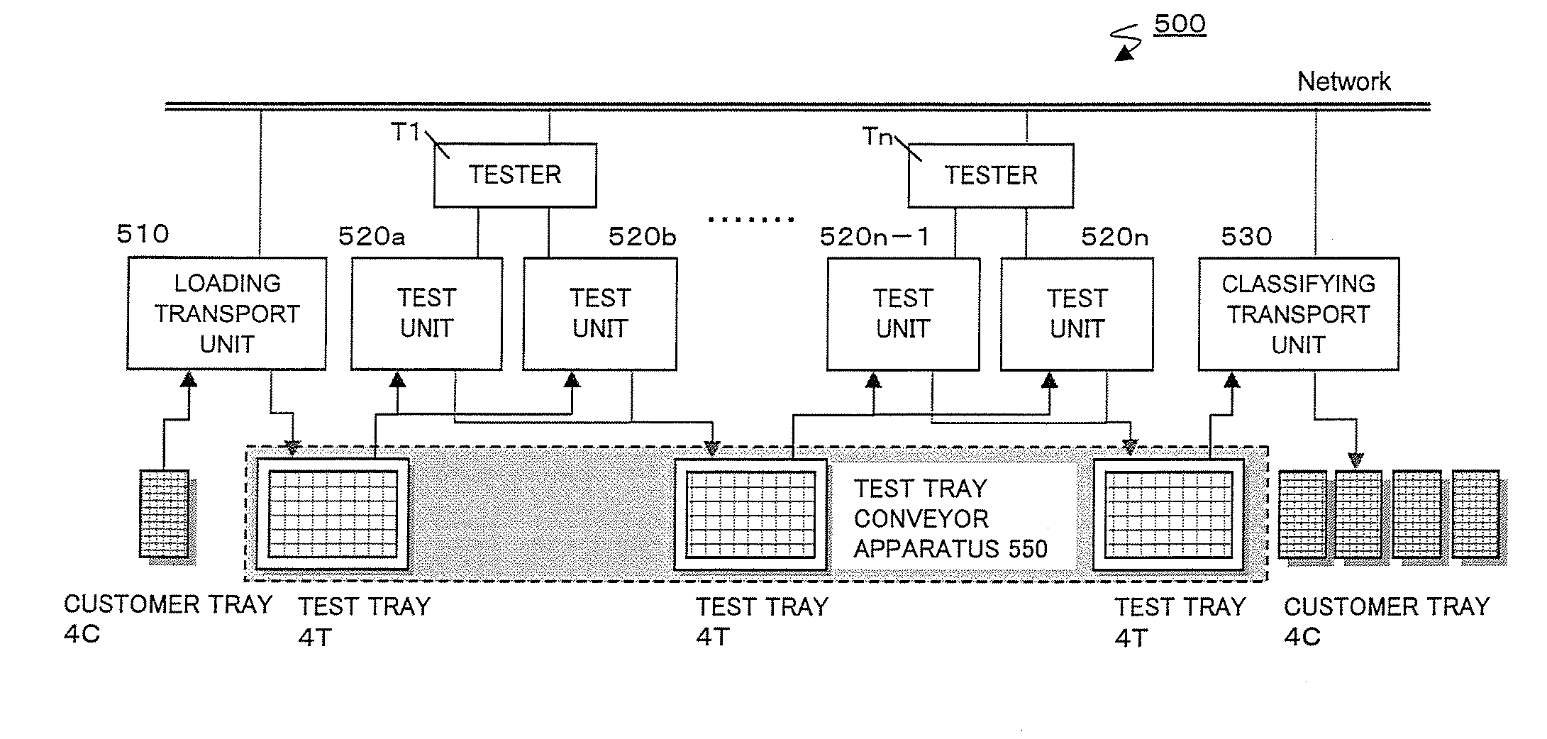
[0042]FIG. 1 to FIG. 6 will be referred to so as to explain a first embodiment of the electronic device test apparatus according to the present invention.

[0043]First, as shown in FIG. 1, the system including the electronic device test apparatus 500 of the present embodiment comprises, from the upstream side, a loading transport unit 510, a plurality of testers T1 . . . Tn, a plurality of test units 520a . . . 520n, and a classifying transport unit 530 in series.

[0044]Each tester T outputs test signals to electronic devices and examines the response signals and is comprised of a test program and a computer for running the same. The tester T is connected through a test signal or other cable to a test head (not shown). This test head is provided with contact units (not shown) for contact with input / output terminals of the electronic devices.

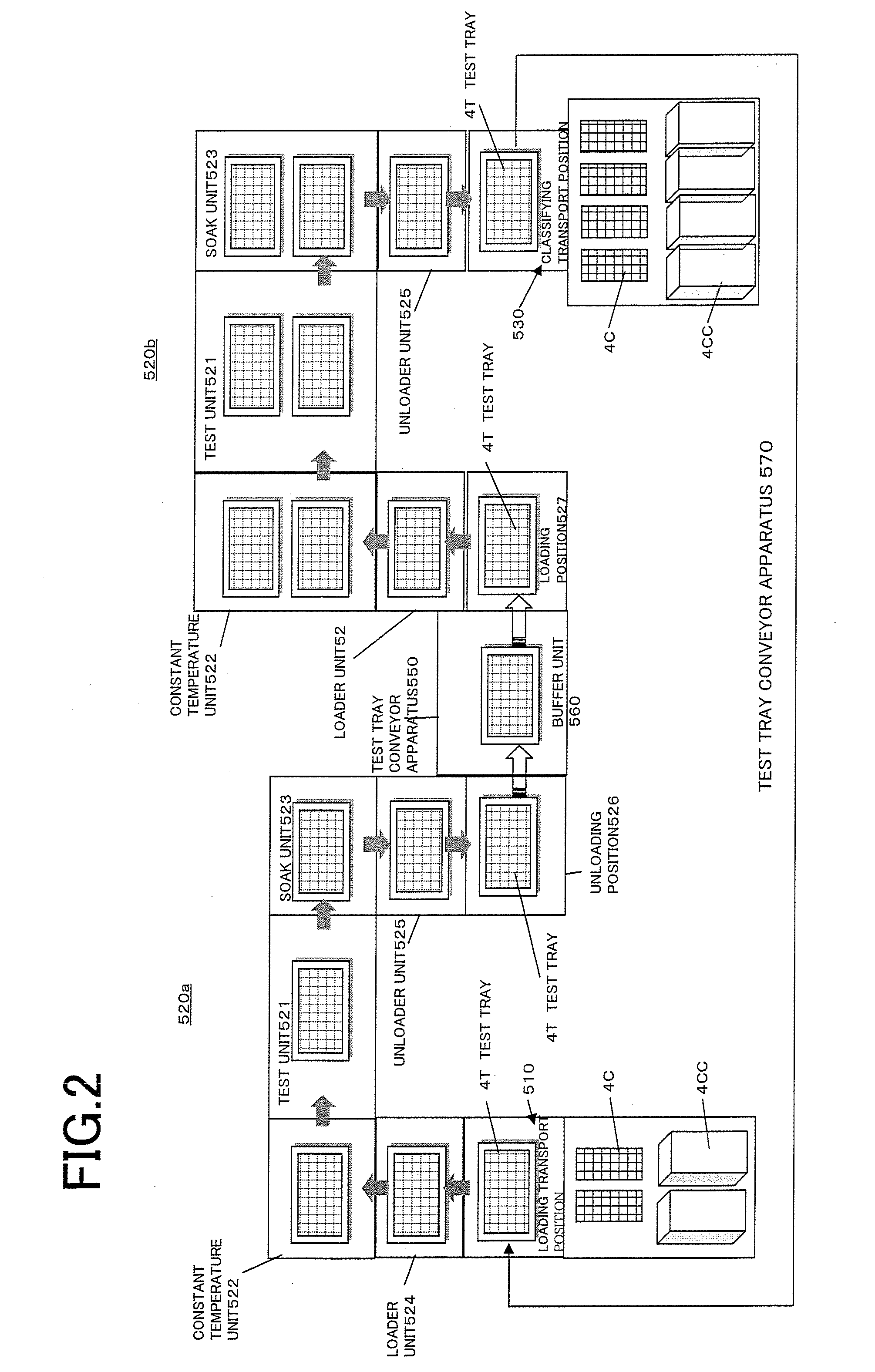
[0045]The test unit 520 has a tester 521 to which the above-mentioned test head is mounted. As shown in FIG. 1, one tester T1 is provided with for ...

second embodiment

[0110]FIG. 12 to FIG. 20 are views of a second embodiment of the electronic device test apparatus according to the present invention.

[0111]In this embodiment, when interchangeably configuring a handling module A comprised of the loader unit 21 and unloader unit 22 as shown in FIG. 12 and a handling module B comprised of the loader unit 21, unloader unit 22, and stocker unit 24 as shown in FIG. 13 for the loader unit 21, unloader unit 22, and stocker unit 24 other than the test unit 1 configured by the constant temperature unit 11, test unit 12, and soak unit 13 shown in FIG. 12 and FIG. 13 and using the test unit 1 for the system of the electronic device test apparatus 500 according to the above-mentioned first embodiment, as shown in FIG. 12, the handling module A is used. Further, when using this as a single electronic device test apparatus, as shown in FIG. 13, the handling module B is used. Due to this, this can be used both for the mass production type test system shown in FIG....


PUM


Abstract

An apparatus having a plurality of test units (520), a loading transport unit (510) transporting a plurality of electronic devices from a customer tray (4C) to a test tray (4T) before being loaded in a test unit, and a classifying transport unit (530) transporting a plurality of electronic devices from a test tray while classifying them to customer trays in accordance with test results, the loading transport unit being provided at least at a frontmost stage of a plurality of test units, the classifying transport unit being provided at least at a rearmost stage of the plurality of test units, the test tray being successively conveyed from the frontmost stage to the rearmost stage of the plurality of test units in the state carrying electronic devices and returned from the rearmost stage test unit to the frontmost stage test unit.

Description

TECHNICAL FIELD[0001]The present invention relates to an electronic device test apparatus for testing a semiconductor integrated circuit device or other various types of electronic devices.BACKGROUND ART[0002]In the process of production of semiconductor devices, an electronic device test apparatus becomes necessary for testing the finally produced IC chip or other electronic device. This type of electronic device is tested by setting the test environment to an ordinary temperature, high temperature, or low temperature environment, inputting a test pattern to the IC chip, operating it in that temperature state, and examining the response pattern. This is because the characteristics of an IC chip have to be guaranteed to enable good operation both under ordinary temperature or a high temperature or low temperature.[0003]A conventional general electronic device test apparatus is comprised of a test head provided with a tester in which a program for transmitting a test pattern and exam...

Claims


Application Information

Patent Timeline
Patent Type & Authority Applications(United States)
IPC IPC(8): H01L21/677
CPCG01R31/2868G01R31/2893G01R31/2865G01R31/31905G01R31/31718G01R31/26H01L22/00
Inventor ITO, AKIHIKOYAMASHITA, KAZUYUKIKOBAYASHI, YOSHIHITO
Owner ADVANTEST CORP
Why Eureka
Try Eureka