

Junction field effect transistor input buffer level shifting circuit
- Summary
- Abstract
- Description
- Claims
- Application Information
AI Technical Summary
Problems solved by technology
Method used
Image

Examples
Embodiment Construction
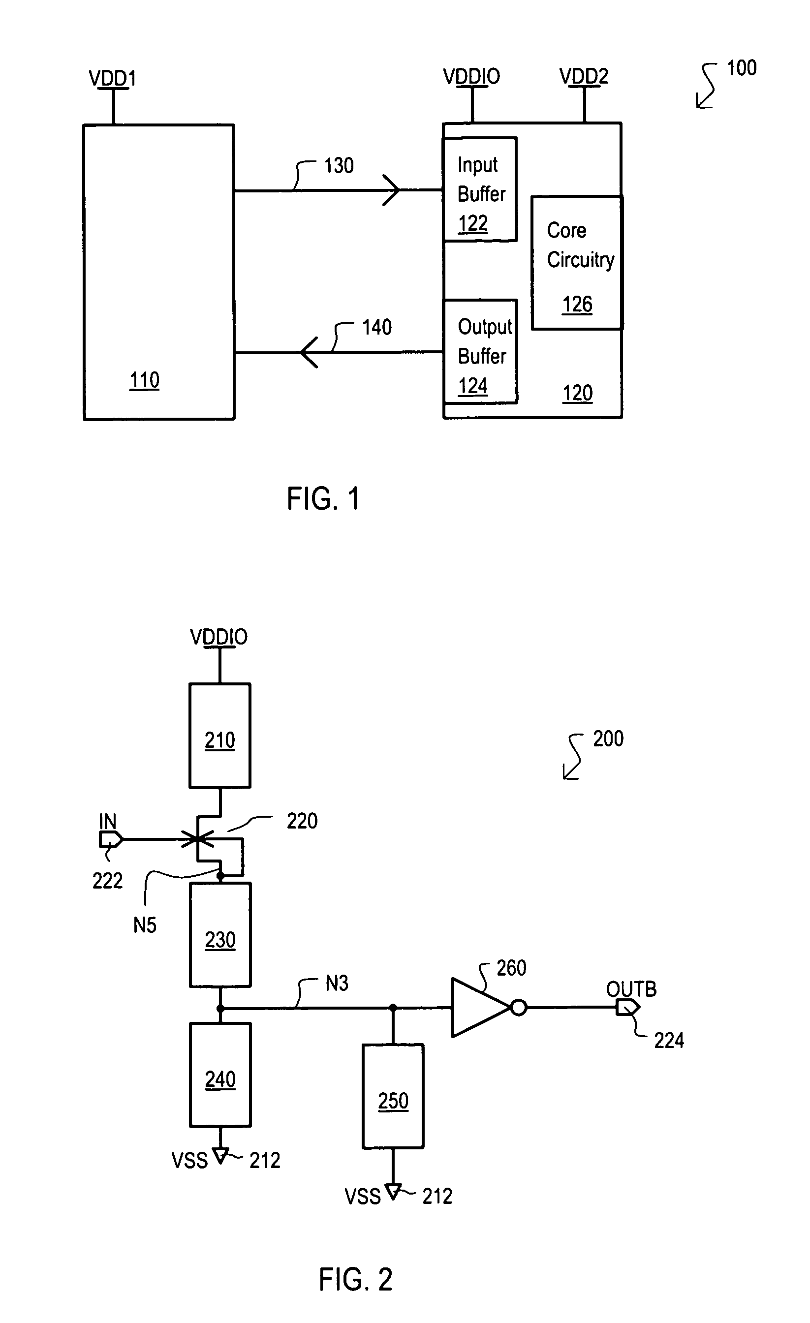
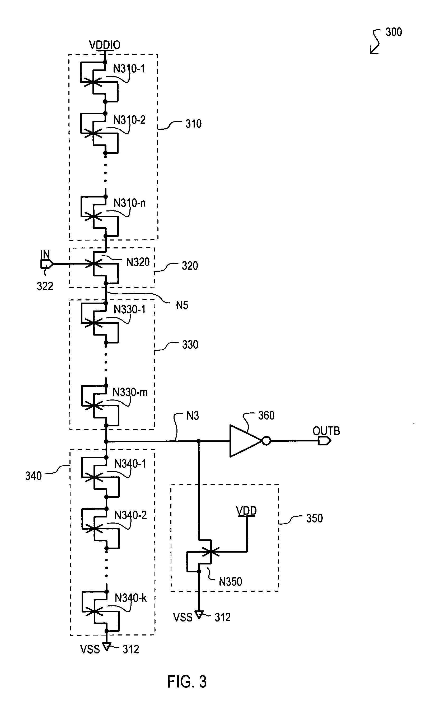
[0012]Various embodiments of the present invention will now be described in detail with reference to a number of drawings. The embodiments show level shifting circuits and methods constructed with junction field effect transistors (JFETs), for example four terminal JFETs of complementary conductivity types (n-channel and p-channel types or PJFETs and NJFETs). Four terminal JFETs can include two control terminals on different sides of a channel region.
[0013]The disclosed embodiments are in contrast to conventional level shifting circuits formed from complementary metal-oxide-semiconductor (CMOS) type technologies, constructed with MOS type transistors.
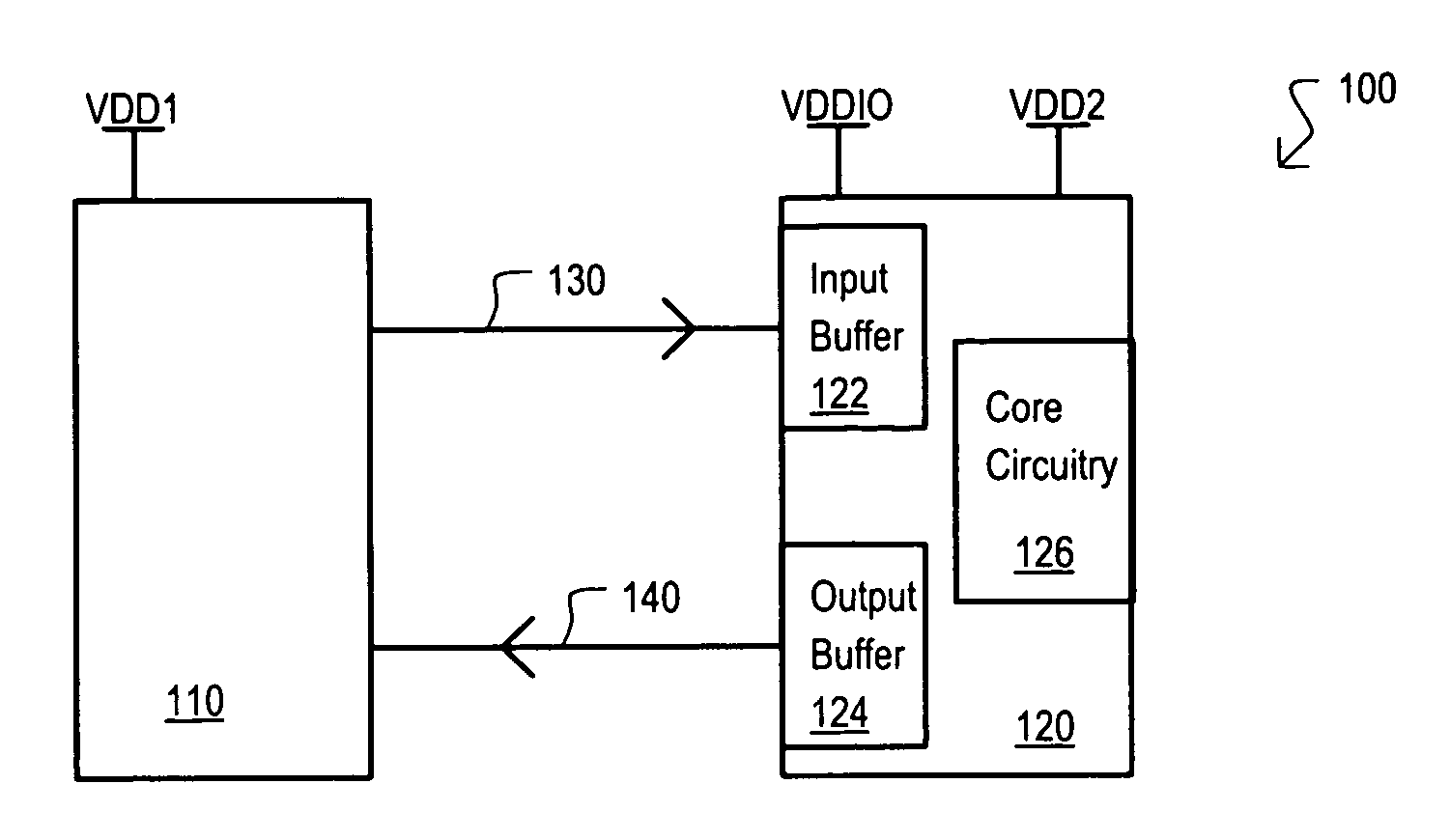
[0014]Referring now to FIG. 1, a block schematic diagram of a system including devices having differing operating voltages according to an embodiment is set forth in a block schematic diagram and given the general reference character 100. System 100 may include a first semiconductor device 110 and a second semiconductor device 120. The ...
PUM
 Abstract
Description
Claims
Application Information