

Semiconductor devices
a technology of semiconductors and devices, applied in the direction of semiconductor devices, basic electric elements, electrical equipment, etc., can solve the problems of difficult wire drawing, inability to achieve a transistor which can perform high-speed switching operations, etc., to achieve high-speed switching operations, reduce gate resistance, and high current density
- Summary
- Abstract
- Description
- Claims
- Application Information
AI Technical Summary
Benefits of technology
Problems solved by technology
Method used
Image

Examples
first embodiment
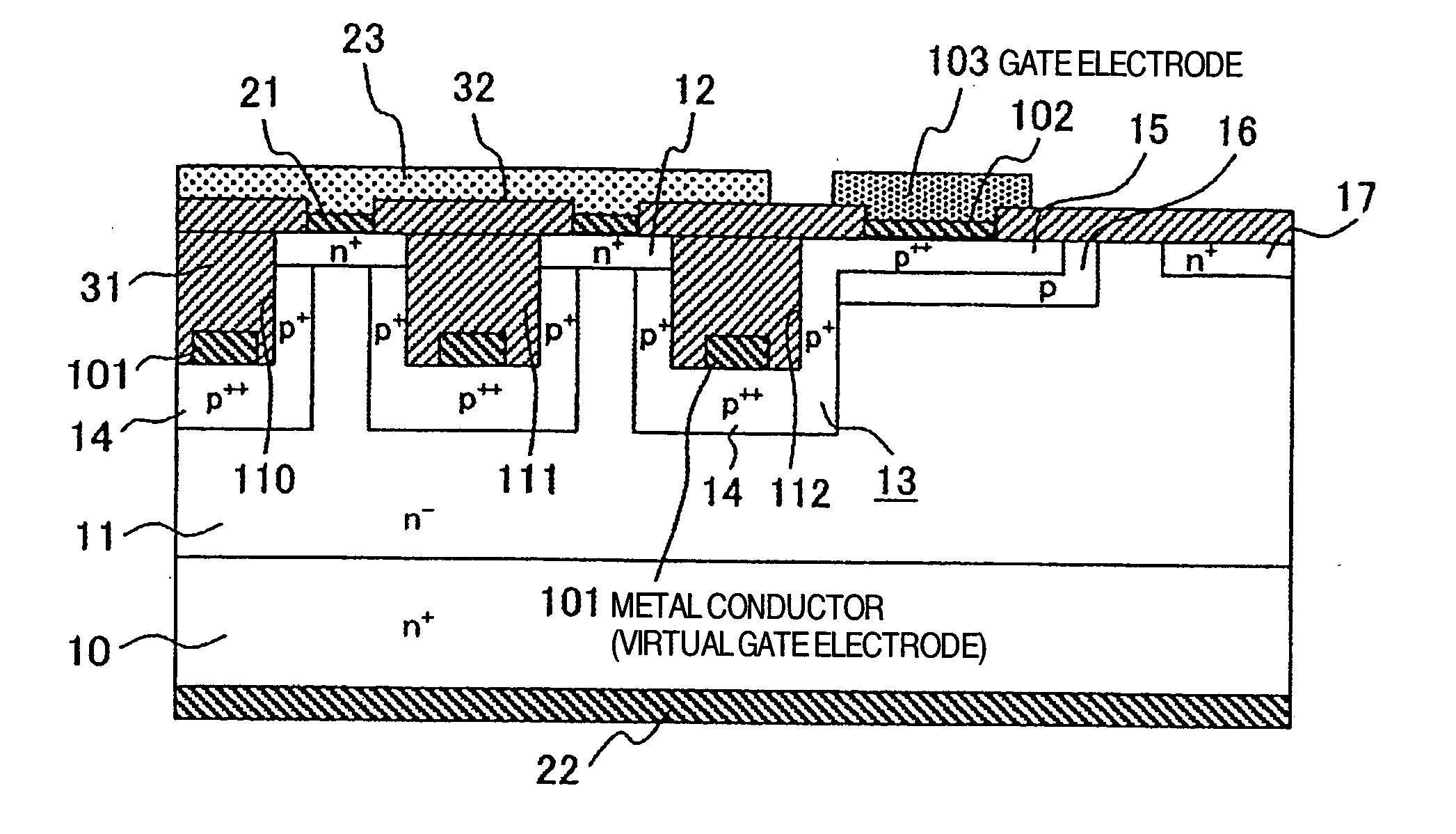
[0029]FIG. 1 is a cross-sectional view illustrating the structure of a static induction transistor (SIT) according to the present invention. In FIG. 1, a semiconductor substrate, the band gap of which is 2.0 eV or more, has a substrate 10 of a first conductivity type n+ (or p+) in a low impurity concentration, which defines a drain region, and a drain electrode 22 formed over the entirety of one surface of the substrate 10. An epitaxial layer (drift layer) 11 is formed on the opposite surface of the substrate 10. The epitaxial layer 11 has a higher impurity concentration than the substrate 10 of the first conductivity type and a low resistance. An n+ source region 12 is formed on the opposite surface of the semiconductor substrate. On the surface of the source region 12, a source contact layer 21 made of nickel is formed in order to form an ohmic contact. An aluminum-made source electrode 23 is disposed on the source contact layer 21. In this embodiment, the aluminum-made source ele...
second embodiment
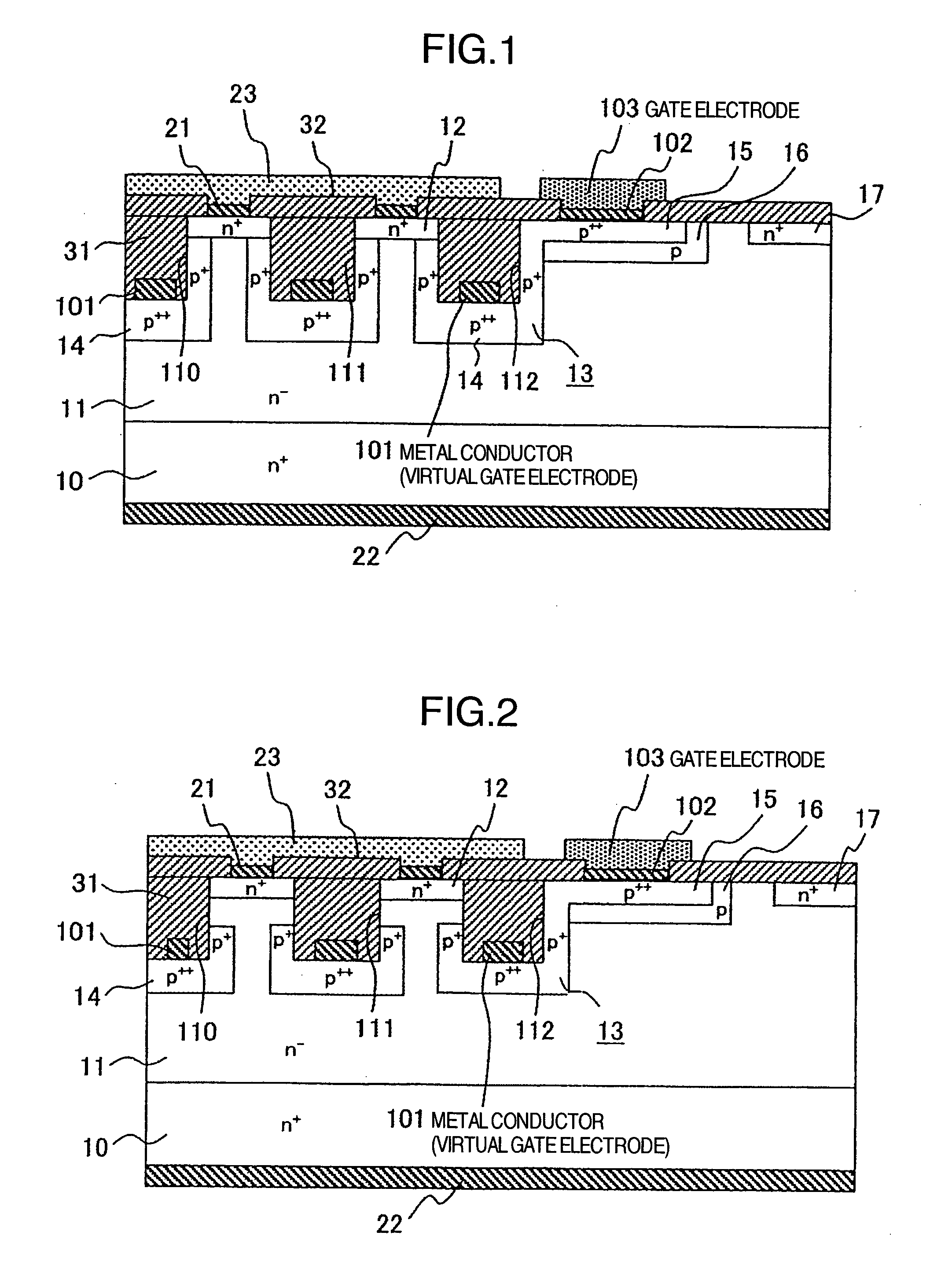
[0035]FIG. 2 is a cross-sectional view generally illustrating the structure of a static induced transistor (SIT) according to the present invention.
[0036] In the present invention, a reduction in channel width is effective for enhancing the blocking effect of the gate, however, the channel need not be reduced in width entirely in the depth direction of the channel. For this reason, the gate region 13 need not be formed over the entire side walls of the grooves. In the second embodiment, the gate region 13 is formed along the bottoms of the trench grooves 110-112 within a range in which the gate region 13 does not reach the source region 12 formed along the opposite surface of the semiconductor substrates. The metal conductor (virtual electrode) 101 is formed on the bottom of each of the trench grooves 110-112 for reducing the gate resistance, and an ohmic contact is established between the p++ gate draw-out layer 14 and each metal conductor 101. Thus, the resulting high-current semi...
third embodiment
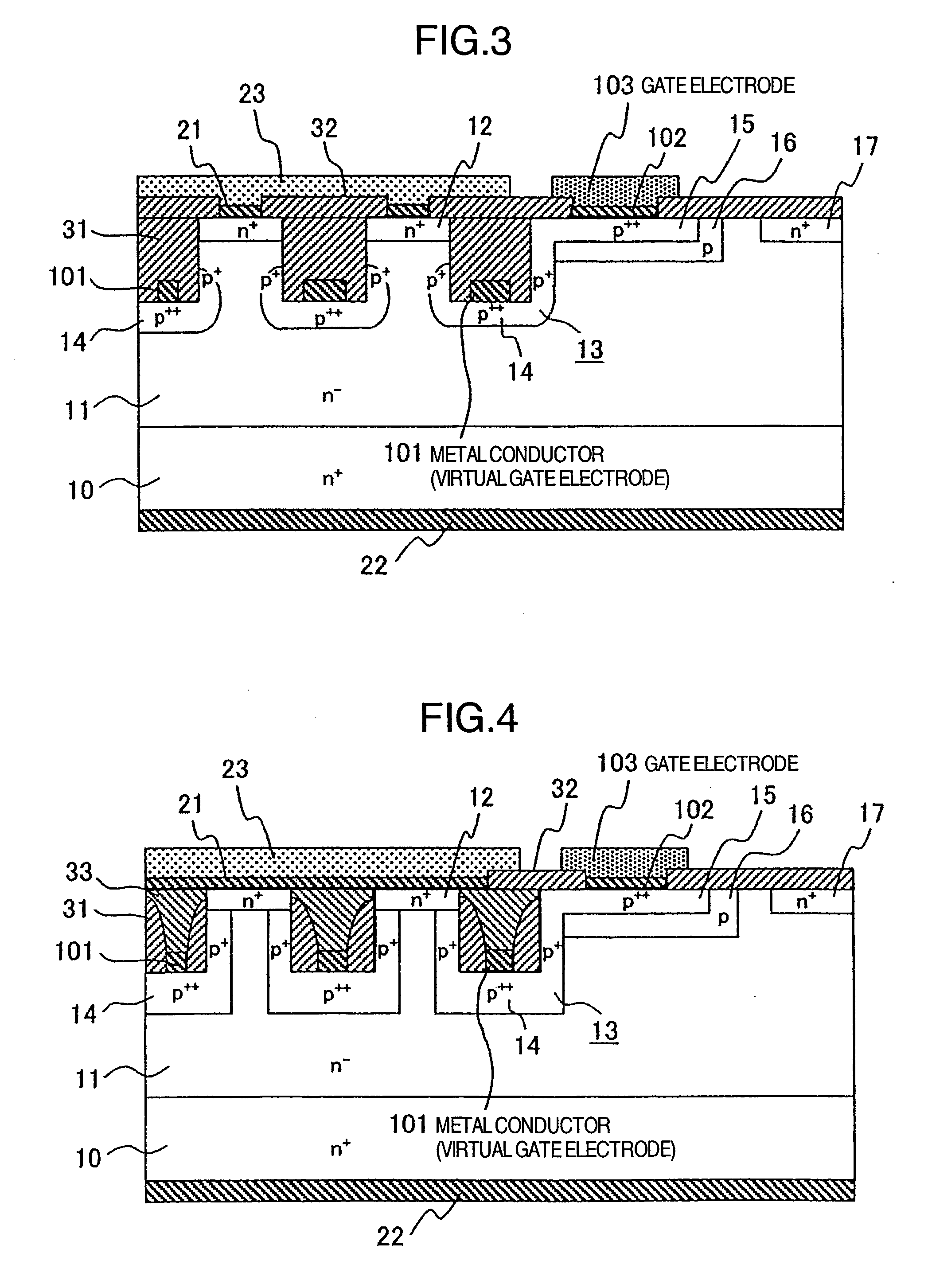
[0037]FIG. 3 is a cross-sectional view generally illustrating the structure of a static induced transistor (SIT) according to the present invention.
[0038] The structure in the third embodiment is substantially the same as that illustrated in FIG. 2 except that the gate region 13 has a rounded contour. In this embodiment, the resulting high-current semiconductor device exhibits high-speed switching characteristics, as is the case with the semiconductor device of the second embodiment illustrated in FIG. 2. The remaining structure is similar to that illustrated in FIG. 1.
[0039]FIG. 4 is a cross-sectional view generally illustrating the structure of a static induced transistor (SIT) according to a fourth embodiment of the present invention. The fourth embodiment differs from the embodiments illustrated in FIGS. 1 to 3 in that the trench grooves are embedded with an insulating film which is composed of a silicon oxide film 31 and a polysilicon film 33 in a two-region structure, and a s...
PUM
 Abstract
Description
Claims
Application Information