Switching semiconductor devices and fabrication process

a technology of semiconductor devices and fabrication processes, applied in the direction of semiconductor devices, basic electric elements, electrical equipment, etc., can solve the problems of unnecessary voltage drop, increase in gate voltage, increase in on-resistance, etc., to avoid an erroneous operation of a jfet

Inactive Publication Date: 2007-05-03
RENESAS ELECTRONICS CORP
View PDF8 Cites 46 Cited by
  • Summary
  • Abstract
  • Description
  • Claims
  • Application Information

AI Technical Summary

Benefits of technology

[0011] Therefore, an object of the present invention is to provide a switching semiconductor device in which, in order to avoid an erroneous operation of a JFET even when gate potential is increased due to noise, a breakd

Problems solved by technology

However, even in the technology disclosed in Patent Document 2 (FIG. 16), unnecessary voltage drop occurs in an ON state at the separation portion, that is, the n− type low-concentration region.
Therefore, a defect, that is, an increase in ON-resistance probably occurs.
As described above, the problems in the above-descri

Method used


Image

  • Switching semiconductor devices and fabrication process
  • Switching semiconductor devices and fabrication process
  • Switching semiconductor devices and fabrication process

Examples


first embodiment

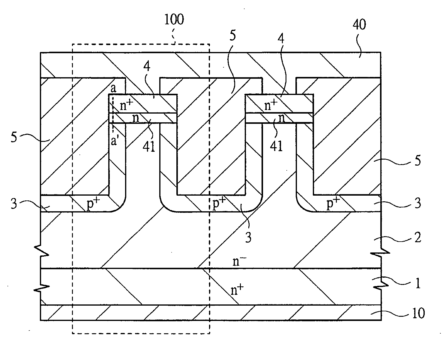
[0044]FIG. 1 is a sectional view of a switching semiconductor device according to a first embodiment of the present invention. The switching semiconductor device according to this embodiment is fabricated by using a semiconductor substrate having opposing first and second surfaces and a band gap of 2.0 eV or more. The switching semiconductor device includes: an n+ type source region 4 with a high impurity concentration extending to the first surface in this semiconductor substrate; an n+ type drain region 1 with a high impurity concentration extending to the second surface in this semiconductor substrate; an n− type drift region 2 with a lower impurity concentration than those of the source region 4 and the drain region 1, which is adjacently formed between the source region 4 and the drain region 1 in the semiconductor substrate; a trench 5 formed to extend to the first surface in this semiconductor substrate; and a p+ type gate region 3 with a high impurity concentration, which de...

second embodiment

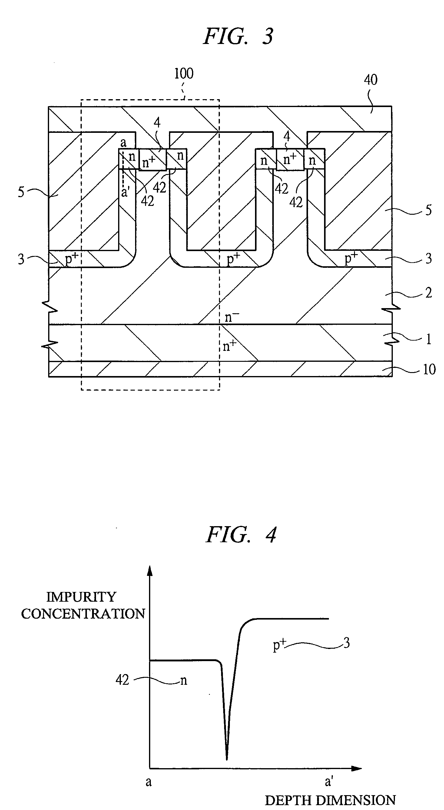
[0047]FIG. 3 is a sectional view of a switching semiconductor device according to a second embodiment of the present invention. In the switching semiconductor device according to this embodiment, a source region 42 with a low impurity concentration is provided around the source region 4 with a high impurity concentration, and a main region through which a current flow is the n+ type source region 4 with a high impurity concentration. Therefore, in this embodiment, a semiconductor device with a lower ON-resistance compared with the first embodiment can be achieved.

[0048] More specifically, the source region includes: n type source regions 42 distributed into a plurality of island regions each surrounded by and in contact with the gate region 3 and having an impurity concentration lower than that of the gate region 3 and higher than that of the drift region 2 at portions in contact with the gate region 3; and the source region 4 adjacent to this source region 42 and having an impurit...

third embodiment

[0050]FIG. 5 is a sectional view of a switching semiconductor device according to a third embodiment of the present invention. In the switching semiconductor device according to this embodiment, a low-resistant gate electrode 30 ohmic-connected to the p+ type gate region 3 provided at the bottom of the trench 33 is formed in a plug shape so as to fill the trench 33. This gate electrode 30 is preferably formed of tungsten W, molybdenum Mo, aluminum Al, nickel Ni, or a compound thereof. Alternatively, the gate electrode 30 can be formed of a low-resistant polysilicon. By this means, since the p+ type gate region 3 is shunted by the low-resistant gate electrode 30, gate resistance components viewed from the gate terminal of the semiconductor device (not shown) are significantly reduced. Accordingly, in this semiconductor device, the voltage fluctuation due to a noise current of the p+ type gate region 3 can be easily suppressed by using a negative gate voltage applied from the gate cir...


PUM


Abstract

A switching semiconductor device is provided, in which a negative gate voltage can be applied to the semiconductor device in an OFF state so as to increase a breakdown voltage of the gate junction without impairing a normally-off function of the semiconductor device and the ON-resistance. The switching semiconductor device is fabricated by using a semiconductor substrate with a band gap of 2.0 eV or more. In a JFET structure where a p+ type gate region and an n type source region are in contact so that a negative gate voltage can be applied, the p+ type gate region and an n+ type source region with a high impurity concentration are disposed with interposing an n type source region with an impurity concentration lower than that of the p+ type gate region and higher than that of a drift region of the JFET therebetween.

Description

CROSS-REFERENCE TO RELATED APPLICATION [0001] The present application claims priority from Japanese Patent Application No. JP 2005-318454 filed on Nov. 1, 2005, the content of which is hereby incorporated by reference into this application. TECHNICAL FIELD OF THE INVENTION [0002] The present invention relates to switching semiconductor devices. More particularly, it relates to a technology effectively applied to a power converter of a switching semiconductor device configured of a junction field effect transistor (JFET) fabricated by using a semiconductor substrate made of silicon carbide (SiC), diamond, gallium nitride (GaN), or the like with a wide band gap of 2 eV or more. BACKGROUND OF THE INVENTION [0003] For example, in a power converter using a semiconductor device, it is required to downsize the power converter without decreasing conversion efficiency. For its achievement, a semiconductor device capable of a high-speed switching operation with low loss is indispensable. Thus...

Claims


Application Information

Patent Timeline
IPC IPC(8): H01L31/111
CPCH01L29/0692H01L29/1608H01L29/2003H01L29/66909H01L29/8083
Inventor WATANABE, ATSUO
Owner RENESAS ELECTRONICS CORP
Why Eureka
Try Eureka