Front contact with high-function TCO for use in photovoltaic device and method of making same

a photovoltaic device and high-function technology, applied in the direction of basic electric elements, electrical apparatus, semiconductor devices, etc., can solve problems such as inefficient performance, and achieve the effects of reducing the potential barrier for holes, low work function, and high work function

Inactive Publication Date: 2008-02-28
GUARDIAN GLASS LLC
View PDF16 Cites 95 Cited by
  • Summary
  • Abstract
  • Description
  • Claims
  • Application Information

AI Technical Summary

Benefits of technology

[0003]Typical TCOs used for certain front contacts of photovoltaic devices are n-type and therefore can create a Schottky barrier at the interface between the TCO and the uppermost semiconductor layer of the photovoltaic device (e.g., p-type silicon based layer) in a reverse direction to the built-in field. This barrier can act as a barrier for holes extracted from the device by the front contact, thereby leading to inefficient performance.
[0004]Thus, it will be appreciated that there exists a need in the art for an improved front contact for a photovoltaic device which can reduce the potential barrier for holes extracted from the photovoltaic device by the front contact.
[0005]I

Problems solved by technology

This barrier can act as a barrier for holes extracted from the devi

Method used


Image

  • Front contact with high-function TCO for use in photovoltaic device and method of making same
  • Front contact with high-function TCO for use in photovoltaic device and method of making same
  • Front contact with high-function TCO for use in photovoltaic device and method of making same

Examples


Embodiment Construction

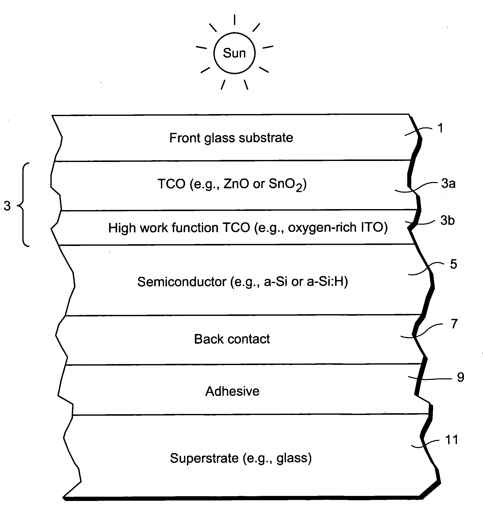
[0012]Photovoltaic devices such as solar cells convert solar radiation and other light into usable electrical energy. The energy conversion occurs typically as the result of the photovoltaic effect. Solar radiation (e.g., sunlight) impinging on a photovoltaic device and absorbed by an active region of semiconductor material (e.g., a semiconductor film including one or more semiconductor layers such as a-Si layers) generates electron-hole pairs in the active region. The electrons and holes may be separated by an electric field of a junction in the photovoltaic device. The separation of the electrons and holes by the junction results in the generation of an electric current and voltage. In certain example embodiments, the electrons flow toward the region of the semiconductor material having n-type conductivity, and holes flow toward the region of the semiconductor having p-type conductivity. Current can flow through an external circuit connecting the n-type region to the p-type region...


PUM


Abstract

This invention relates to a front contact for use in an electronic device such as a photovoltaic device. In certain example embodiments, the front contact of the photovoltaic device includes a low work-function transparent conductive oxide (TCO) of a material such as tin oxide, zinc oxide, or the like, and a thin high work-function TCO of a material such as oxygen-rich ITO (indium tin oxide) or the like. The high-work function TCO is located between the low work-function TCO and the uppermost semiconductor layer of the photovoltaic device so as to provide for substantial work-function matching between the low work-function TCO and the high work-function uppermost semiconductor layer of the device in order to reduce a potential barrier for holes extracted from the device by the front contact.

Description

[0001]This invention relates to a photovoltaic device including a front contact. In certain example embodiments, the front contact of the photovoltaic device includes a low work-function transparent conductive oxide (TCO) of a material such as tin oxide, zinc oxide, or the like, and a thin high work-function TCO of a material such as oxygen-rich ITO (indium tin oxide) or the like. The high-work function TCO is located between the low work-function TCO and the uppermost semiconductor layer of the photovoltaic device so as to provide for substantial work-function matching between the low work-function TCO and the high work-function uppermost semiconductor layer of the device in order to reduce a potential barrier for holes extracted from the device by the front contact.BACKGROUND AND SUMMARY OF EXAMPLE EMBODIMENTS OF INVENTION[0002]Photovoltaic devices are known in the art (e.g., see U.S. Pat. Nos. 6,784,361, 6,288,325, 6,613,603, and 6,123,824, the disclosures of which are hereby inc...

Claims


Application Information

Patent Timeline
IPC IPC(8): H01L31/00
CPCH01L31/022466H01L31/022475H01L31/022483
Inventor KRASNOV, ALEXEY
Owner GUARDIAN GLASS LLC
Why Eureka
Try Eureka