Process and apparatus for joining at least two elements

a technology of two elements and processes, applied in the direction of laser beam welding apparatus, electrical apparatus, printed circuit manufacturing, etc., can solve the problems of high thermal load of components to be soldered during reflow soldering, high soldering temperature, and increased temperature of micro-electronic components

Inactive Publication Date: 2008-02-28
HUMMELT STEFAN
View PDF11 Cites 12 Cited by
  • Summary
  • Abstract
  • Description
  • Claims
  • Application Information

AI Technical Summary

Problems solved by technology

Although a high throughput can be achieved using reflow soldering, the components to be soldered encounter a high thermal load during reflow soldering.
However, as the integration level and the functionality is ever increasing, micro-electronic components become more and more temperature-sensitive.
However, lead-free soldering, which is prescribed in the future by WEEE, usually causes higher soldering temperatures, which can easily be higher by about 20 K, which further increases the thermal load during soldering.
Due to the higher melting temperature of antimony (Sb), this causes higher soldering temperatures, which also increases the thermal load for components.
Other soldering methods, e.g. a wave-soldering process cannot solve the above problems.
The use of robotics for deflecting beams causes relatively long welding or soldering times, which is not suitable in the mass production of electronic devices.
The processing speed thus accomplished is, however, not sufficient for the production of electronic devices with high throughput, because such a soldering process is also carried out in a sequential manner and lasts for at least 0.5 sec. to about 2 sec.
If one would increase the total number of scanners used in this method, this would require a very complex control of the scanners which would increase the production costs.
Comparable problems also occur in the processing of substrates, e.g. for forming a plurality of holes, blind holes and / or of preweakened zones in a pre-determined geometric configuration.
The mechanical inertia of the scanner mirror inherently limits the processing speed and increases the costs for maintenance.
The processing speed is particularly limited by the inertia of the scanner mirrors, if preweakened zones or perforations are to be formed at locations on a substrate which are far away from each other.
However, this further increases the processing costs.

Method used


Image

  • Process and apparatus for joining at least two elements
  • Process and apparatus for joining at least two elements
  • Process and apparatus for joining at least two elements

Examples


Embodiment Construction

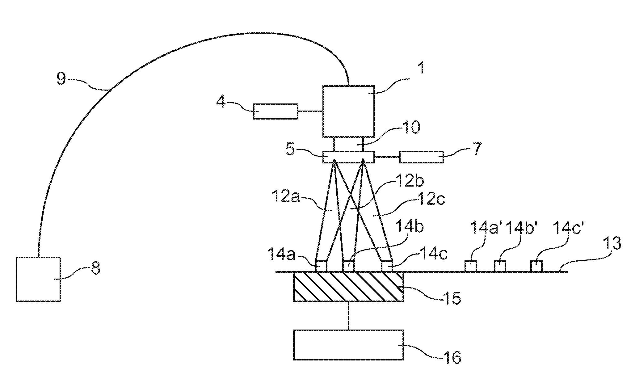
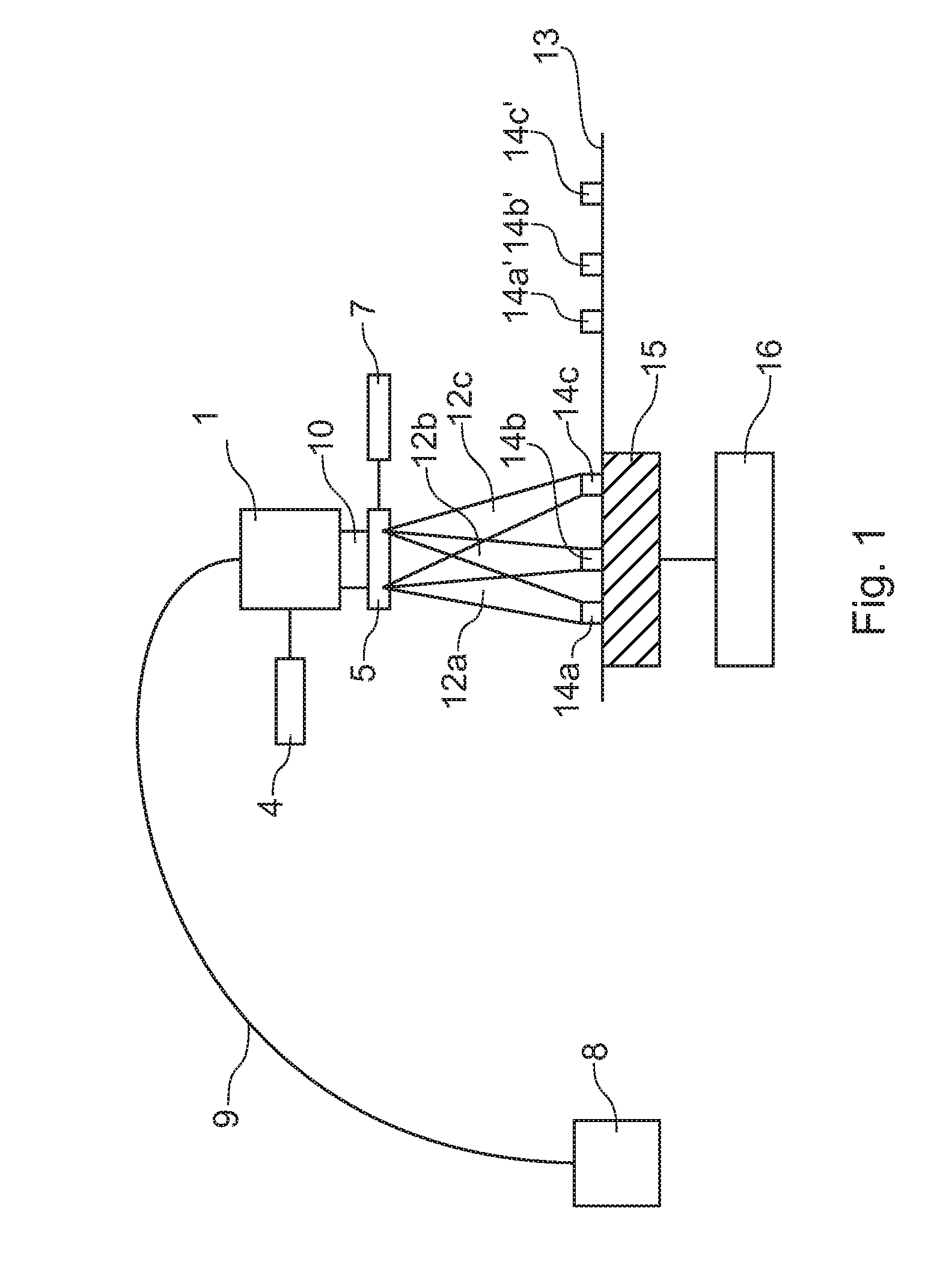
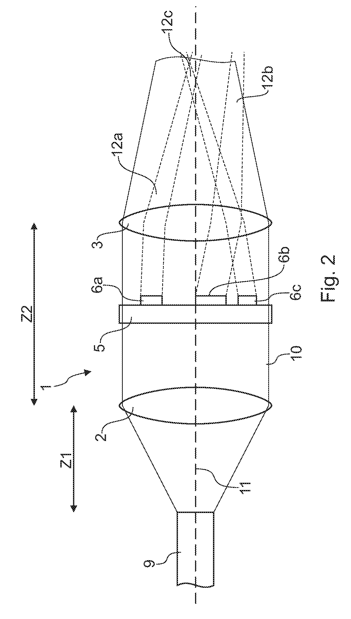
[0044]Referring to FIG. 1 the laser beam of a diode laser 8 is coupled into an optical fiber 9 and is directed towards an apparatus comprising a processing head supporting an imaging optics 1 with an associated diffractive optical element (DOE) 5. The input light beam 10 is divided into a plurality of partial light beams 12a-12c by the imaging optics 1. At the same time, these partial light beams 12a-12c are focused. The distance between the processing head and the printed circuit board (PCB) 13 is therefore adjusted in accordance with the focal length of the imaging optics 1 and the desired diameter of the beam spots on the printed circuit board 13. E.g. a distance between the processing head and the work piece to be processed of the order of about 10 cm to about 50 cm has been implemented. According to FIG. 1, a plurality of components (not shown) are disposed on the printed circuit board 13 in a periodic configuration, of which only respective three contact pins 14a, 14b, 14c for...


PUM

PropertyMeasurementUnit
diameteraaaaaaaaaa
diameteraaaaaaaaaa
surface tensionaaaaaaaaaa

Abstract

Process and apparatus for joining at least two elements, in particular an electronic component such as an LED with a substrate, such as a PCB. An imaging means divides a light beam into a plurality of partial light beams and images these partial light beams, forming a plurality of discrete light spots, which form a plurality of discrete material joining portions. The light beam is divided using a diffractive optical element (DOE) also enabling a beam shaping and beam processing. A plurality of material joining portions can be formed simultaneously enabling a high process rate. The method is suited for laser soldering of components, which are not exposed to high thermal loads, e.g. for forming electrical contacting portions of LEDs. These discrete light spots can also be used for material processing, in particular for simultaneously forming a plurality of preweakened material zones or perforations in a substrate.

Description

RELATED APPLICATIONS[0001]The present application is a continuation-in-part of and claims priority under 35 U.S.C. §120 to U.S. application Ser. No. 11 / 828,377, filed on Jul. 26, 2007, which is in turn related to and claims benefit under 35 U.S.C. § 119(e) to U.S. Provisional Application No. 60 / 840,199, filed on Aug. 25, 2006, both of which are entitled “Process and Apparatus for Joining at Least Two Elements”, the whole content of both of which are hereby incorporated by reference.FIELD OF THE INVENTION[0002]The present invention relates in general to joining or connecting of two elements, in particular by means of a material joining, most preferably using soft-soldering, and relates in particular to a method for contacting of electronic or micro-electronic components using soft-soldering. A related further aspect of the present invention generally relates to a method for processing a substrate using laser beams, in particular for processing web-like or sheet-like materials of arbi...

Claims


Application Information

Patent Timeline
Patent Type & Authority Applications(United States)
IPC IPC(8): B23K26/20
CPCB23K1/0056B23K26/067B23K26/0673H05K2203/107H05K3/3421H05K3/3494B23K26/0838
Inventor HUMMELT, STEFAN
Owner HUMMELT STEFAN
Why Eureka
Try Eureka