

Low loss electrical delay line
a delay line and low loss technology, applied in the direction of waveguides, basic electric elements, semiconductor devices, etc., can solve the problems of time further increasing the insertion loss, the transistor fabrication process (mmic) is expensive and requires high resolution, and the inability to provide all the desired attributes, etc., to achieve simplified delay line solution, reduce the dielectric loss, and simplify the effect of delay lin
- Summary
- Abstract
- Description
- Claims
- Application Information
AI Technical Summary
Benefits of technology
Problems solved by technology
Method used
Image

Examples
Embodiment Construction
[0028]In the following detailed description of the preferred embodiments, reference is made to the appended drawings which form a part hereof, and within which are shown, by way of illustration, specific embodiments by which the invention may be practiced. It is to be understood that other embodiments may be utilized and structural changes may be made without departing from the spirit and scope of the invention. The following detailed description is, therefore, not to be taken in a limiting sense, and the scope of the present inventions is defined only by the appended claims.
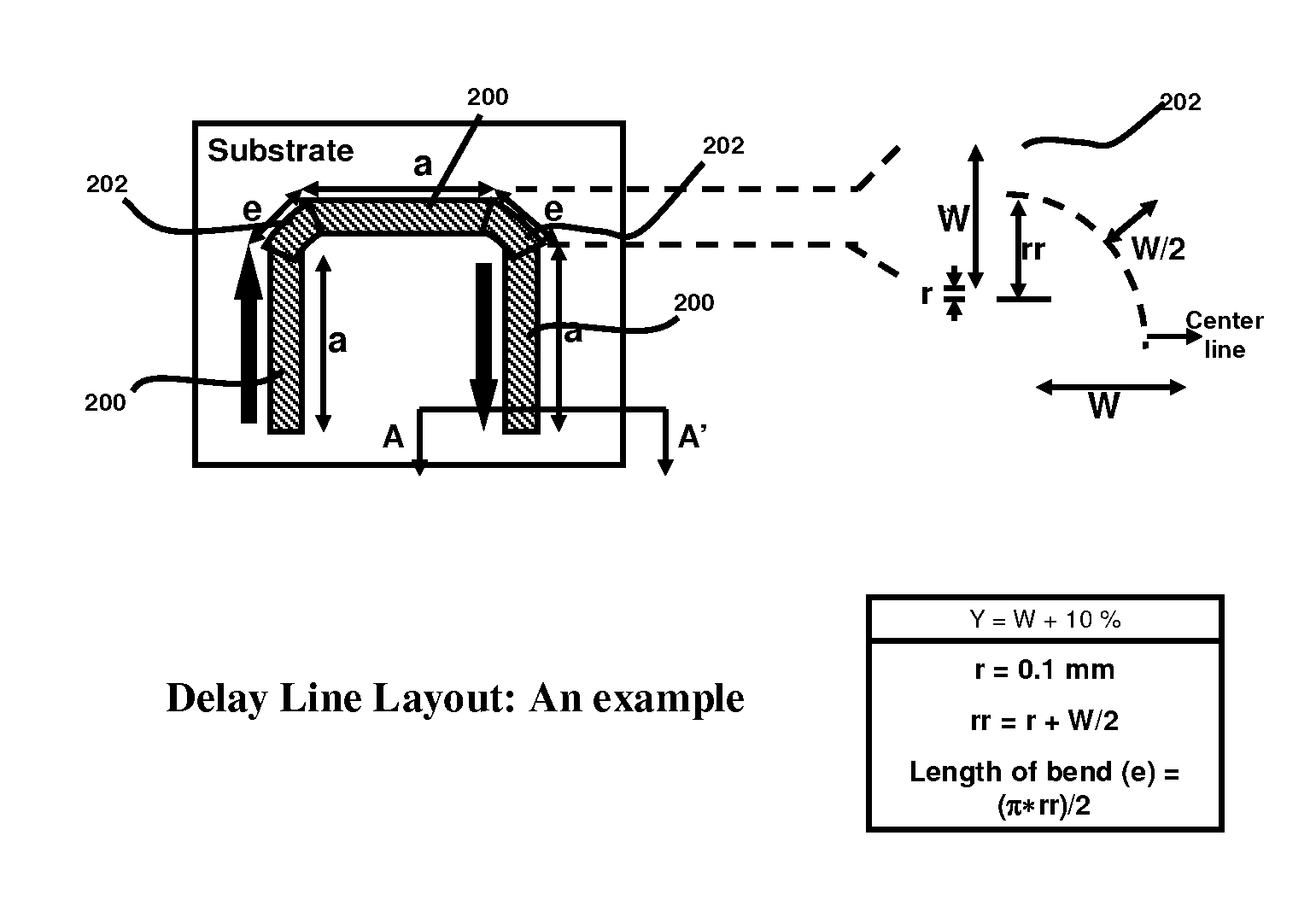
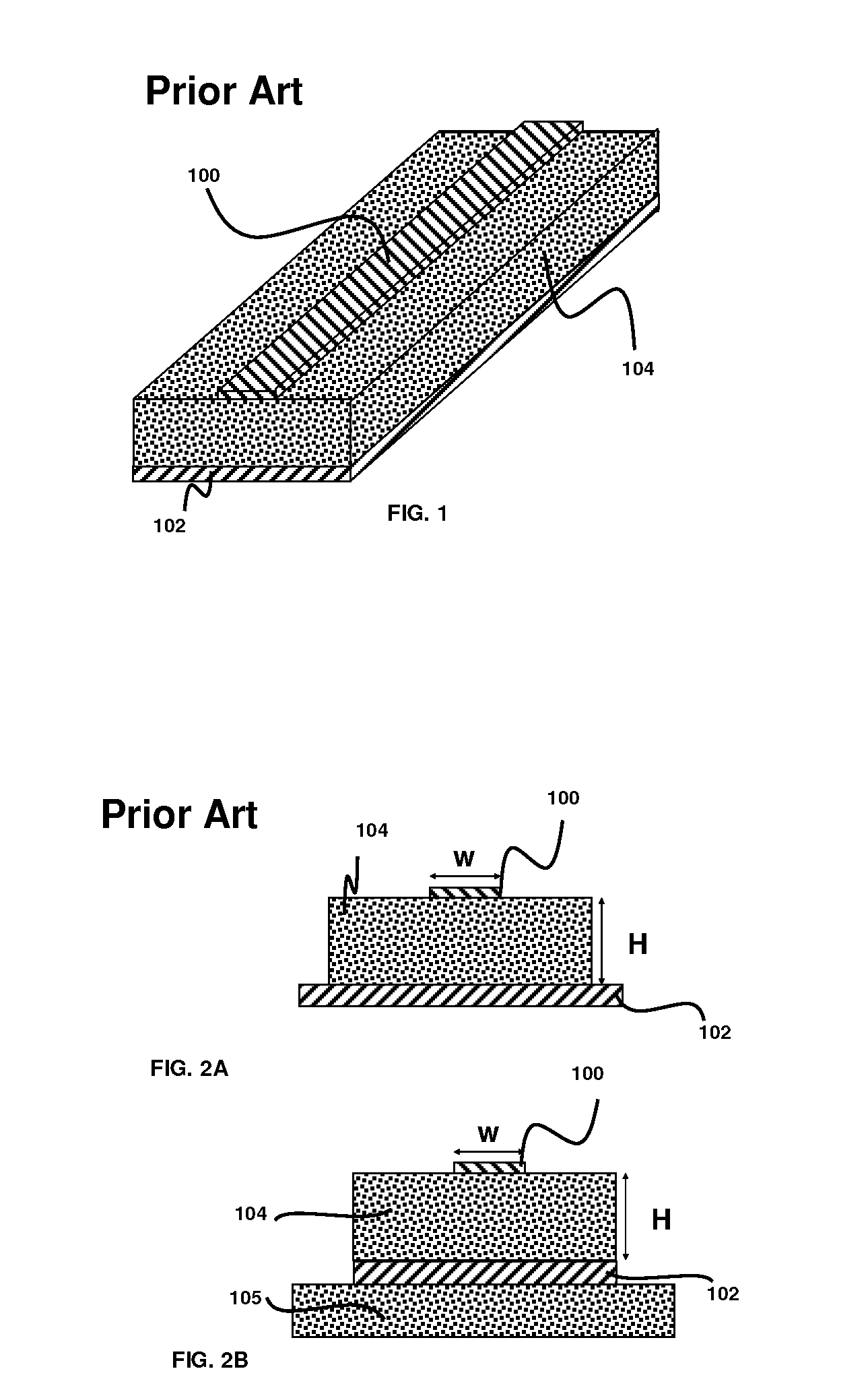
[0029]A single delay line can be as simple as a straight line such as the line shown in FIG. 1, or more complex, including many bends as shown in FIG. 8A-8D. Multiple delay lines can be chained together as shown in FIG. 8E to create a controlled, variable delay line system at the cost of whatever loss is introduced by the switches.
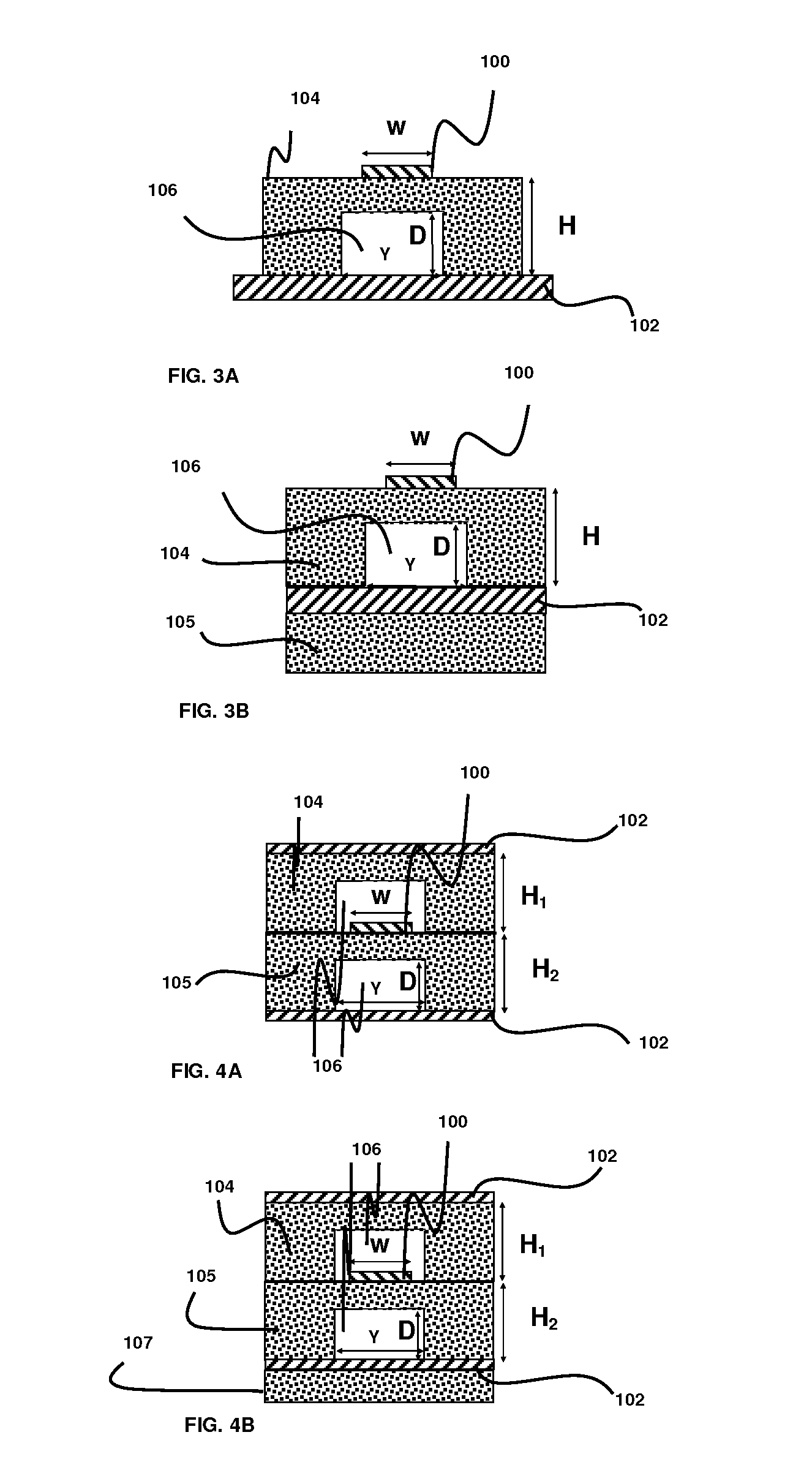
[0030]The structure of each delay line can vary quite significantly. These varianc...
PUM
 Abstract
Description
Claims
Application Information