Measuring Diffractive Structures By Parameterizing Spectral Features

Inactive Publication Date: 2008-02-28
ADVANCED METROLOGY SYST
View PDF3 Cites 35 Cited by
  • Summary
  • Abstract
  • Description
  • Claims
  • Application Information

AI Technical Summary

Benefits of technology

[0018] In another aspect, the invention features an apparatus including a source of electromagnetic radiation of exposing a structure thereto, as well as a detector for measuring a spectrum based on the exposure, detecting characteristics of the measured spectrum that vary identifiably with at least one structural parameter over a range of values of the at least one structural parameter, and comput

Problems solved by technology

The second problem is the “inverse” problem: given a measured spectrum, finding the values of the model parameters which would produce, in simulation, a desired fit to the measured spectrum.
The inverse problem is commonly encountered in many areas of science and engineering.
For measurements of structures using optical spectroscopy, the complexity of the spectrum simulation increases when the optical wavelength is comparable to a characteristic lateral dimension of the structure, e.g., within a factor of 10, or even within a factor of 100.
In this case, the effects of optical diffraction be

Method used


Image

  • Measuring Diffractive Structures By Parameterizing Spectral Features
  • Measuring Diffractive Structures By Parameterizing Spectral Features
  • Measuring Diffractive Structures By Parameterizing Spectral Features

Examples


Example

Example 1

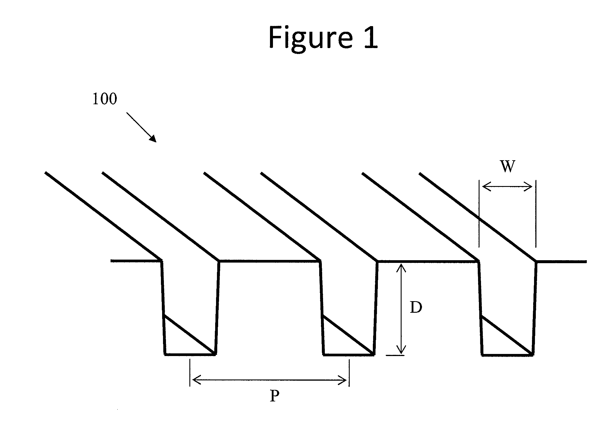
[0048]FIG. 1 illustrates an array of linear trenches 100 etched in a substrate, e.g., a silicon substrate, with array pitch P of 1.5 micrometers (μm), trench depth D of 1.0 μm, and trench width W of 0.4 μm. This structure may occur, for example, in the fabrication of some power metal-oxide-semiconductor field-effect transistor (“MOSFET”) devices.

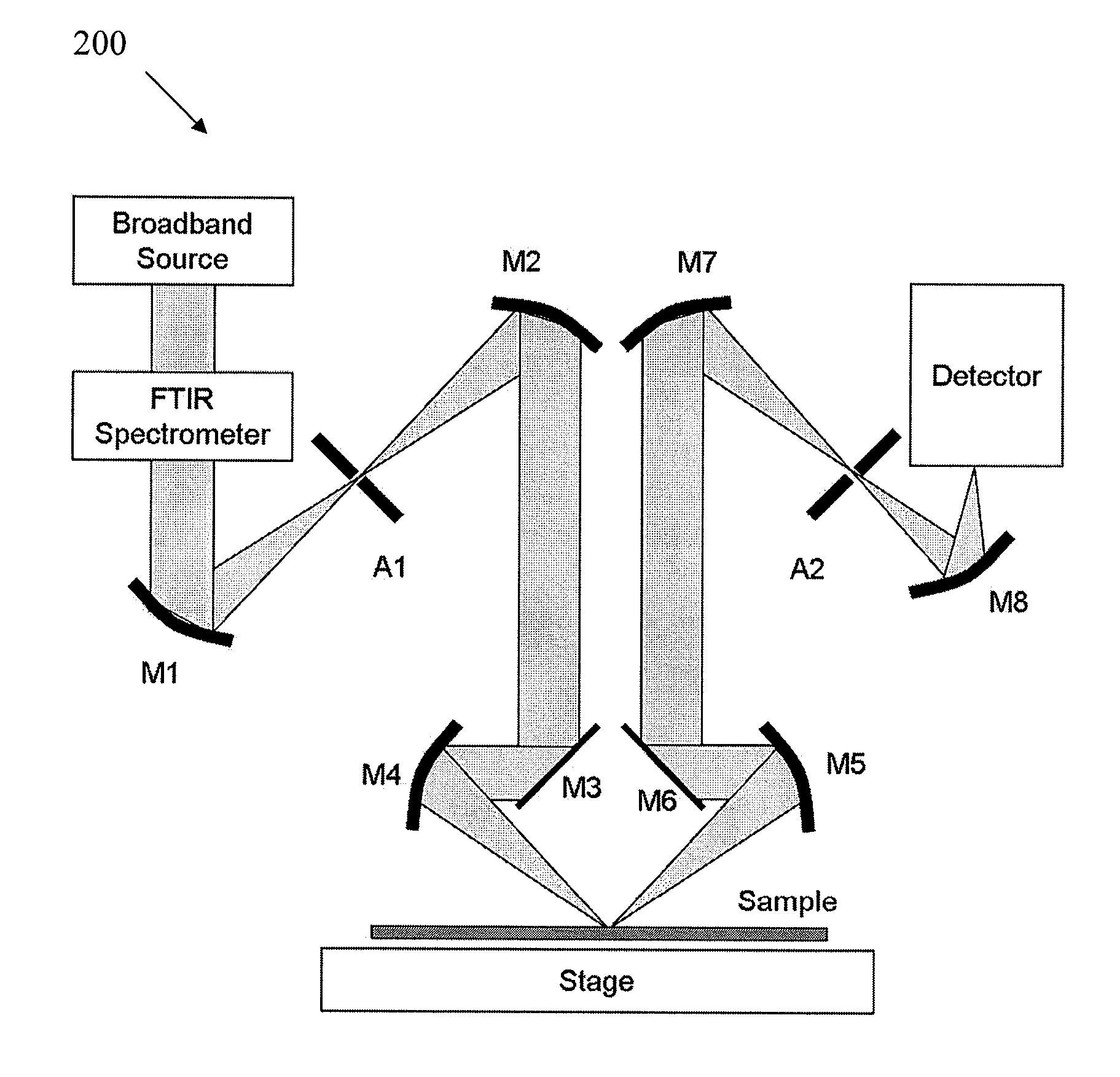
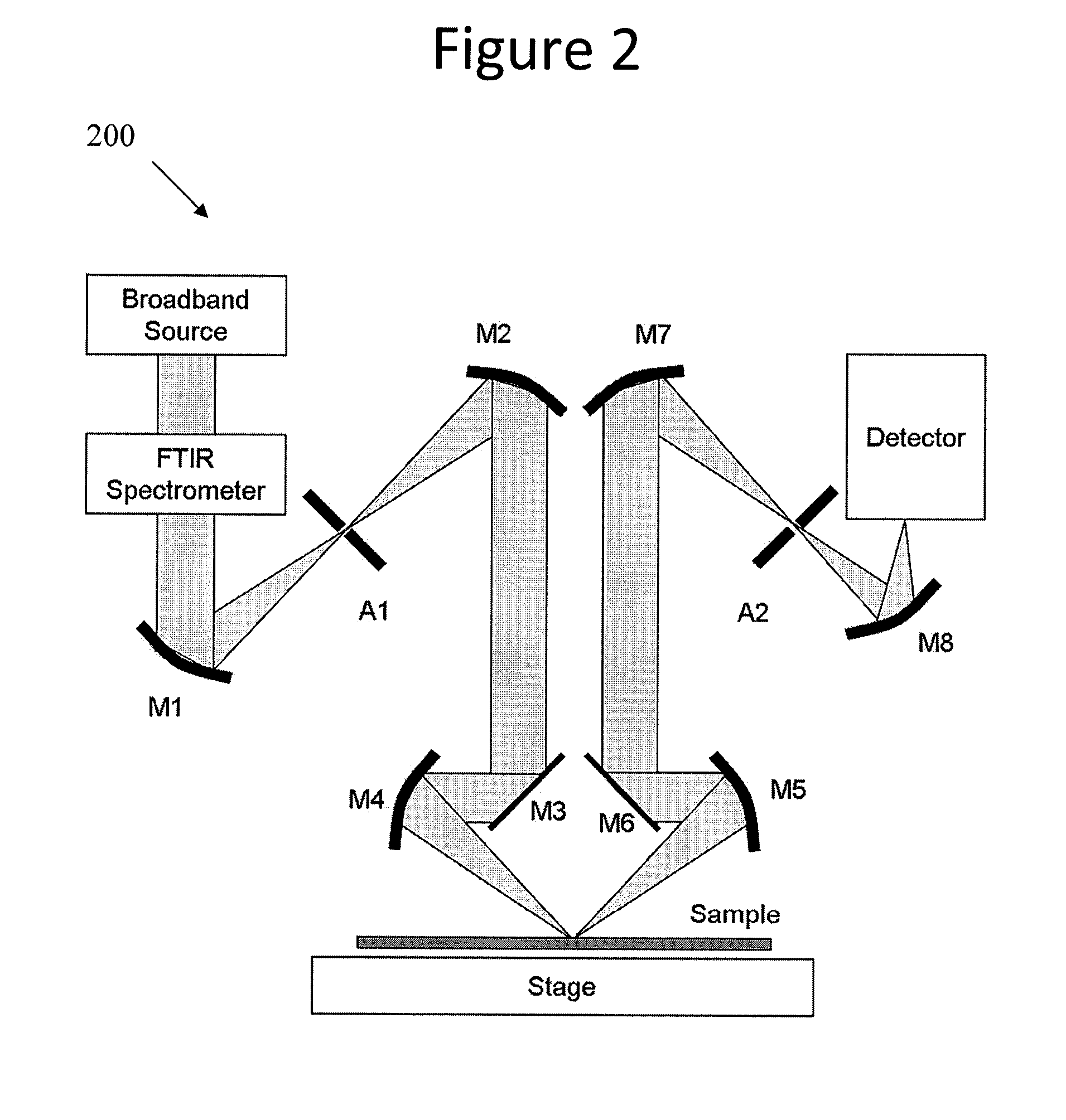
[0049] Array 100 is measured with a suitable measurement instrument 200, e.g., the IR3000 system mentioned above. This instrument has a wavelength range of 1.4 to 20 μm (corresponding to a wavenumber range of 500 to 7000 cm−1), and measures the reflectance spectrum of the sample at a 45° angle of incidence. The instrument design is based on a broadband light source coupled with an FTIR spectrometer and an optical system for illuminating the sample and collecting the reflected light, as shown in FIG. 2. On its path from the light source to the detector, the optical radiation is reflected by a series of mirrors M1-M8 and travels thr...

Example

Example 2

[0059] A second example illustrates the utility of embodiments of the invention for more complex structures. FIG. 8 depicts a recessed linear trench structure 800 formed in an undoped epitaxial silicon layer 810 on a doped silicon substrate 820. Structure 800 is formed by etching trenches into the layer 810, coating the trenches with oxide 830, filling with polysilicon 840, and then etching polysilicon 840 to leave a recess 850 extending beneath the top plane of oxide 830. The pitch P is approximately 4.0 μm, with other dimensions approximately in proportion as indicated on the figure. Structure 800 may be found, for example, during formation of power semiconductor devices.

[0060] It is desired to measure the recess depth RD of structure 800 by analysis of its infrared reflectance spectrum. Due to the magnitude of the pitch P, the reflectance spectrum in the infrared is dominated by diffraction effects, and RCWA or a similar method is utilized to simulate model spectra. Su...


PUM


Abstract

Structures are characterized by exposing a sample to optical radiation, measuring a spectrum associated with the exposure, detecting at least one characteristic parameter in the measured spectrum, and computing at least one structural parameter based on the at least one characteristic parameter.

Description

CROSS-REFERENCE TO RELATED APPLICATIONS [0001] This application claims the benefit of and priority to U.S. Provisional Application Ser. No. 60 / 823,685, filed Aug. 28, 2006, and U.S. Provisional Application Ser. No. 60 / 903,166, filed Feb. 23, 2007, the entire disclosures of which are hereby incorporated by reference.FIELD OF THE INVENTION [0002] The technology disclosed herein relates to measuring the dimensions of structures formed in the fabrication of devices such as integrated circuits. BACKGROUND [0003] The fabrication of semiconductor devices for integrated circuits typically involves generating dense arrays of three-dimensional structures. For example, a workpiece consisting of a semiconductor substrate or a substrate with one or more deposited film layers may be etched to form arrays of linear trenches, cylindrical cavities, or other shapes. We collectively refer to such structures as “trenches” or “trench arrays,” regardless of geometry. These features may be filled with a f...

Claims


Application Information

Patent Timeline
IPC IPC(8): G01B11/00
CPCG01B11/22G01B11/24H01L21/67253G01N21/4788G01N21/956G01N21/274
Inventor MAZNEV, ALEXEIDURAN, CARLOS A.GOSTEIN, MICHAELMAZURENKO, ALEXANDERMERKLIN, GREGORY T.ROSENTHAL, PETERBONANNO, ANTHONY S.
Owner ADVANCED METROLOGY SYST
Why Eureka
Try Eureka