Quantum dot based optoelectronic device

a quantum dot and optoelectronic technology, applied in the field of quantum dot based optoelectronic devices and optoelectronic devices, can solve the problem of high density of dislocation in layers of sufficient thickness for optoelectronic applications, and achieve the effect of commercial longevity and good performance characteristics

Active Publication Date: 2008-03-06
RGT UNIV OF CALIFORNIA
View PDF14 Cites 7 Cited by
  • Summary
  • Abstract
  • Description
  • Claims
  • Application Information

AI Technical Summary

Benefits of technology

[0012] It is an object of the invention to provide a method of fabricating Si-based optoelectronic devices having optically active regions formed from compound semiconductor materials. Devices based on such hetero-structures (e.g., lattice mismatch) will have commercial longevity and good performance characteristics. Exemplary products which may be produced in accordance with the methods described herein include Si-based optical transceiver chips, laser diodes, light emitting diodes, and photodetectors.

Problems solved by technology

This is in contrast with film-based approaches in which much more material is needed to achieve the level of optical activity, as a result, the lattice mismatch between the compound semiconductor material and silicon causes a high density of dislocation in layers of sufficient thickness for optoelectronic applications.

Method used


Image

  • Quantum dot based optoelectronic device
  • Quantum dot based optoelectronic device
  • Quantum dot based optoelectronic device

Examples


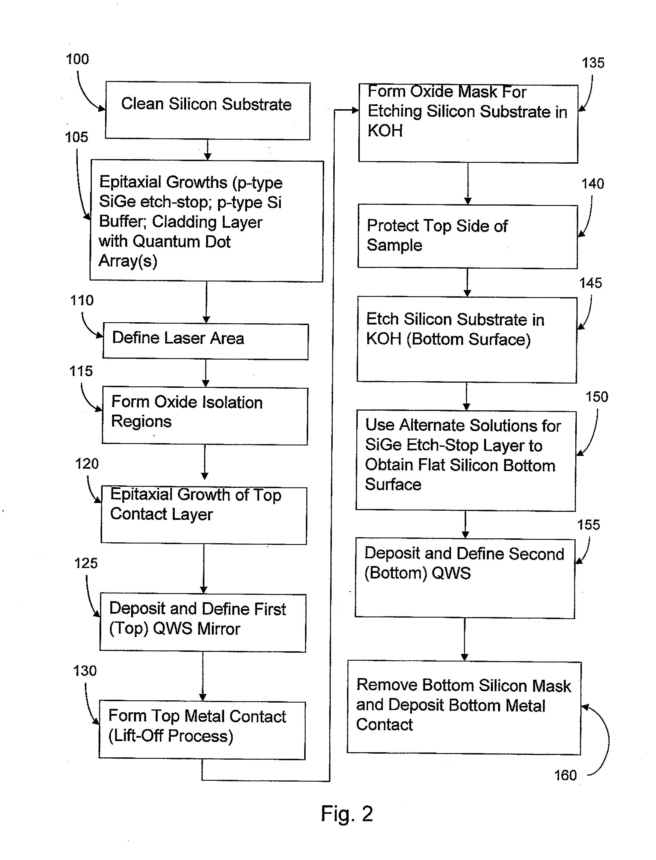
Embodiment Construction

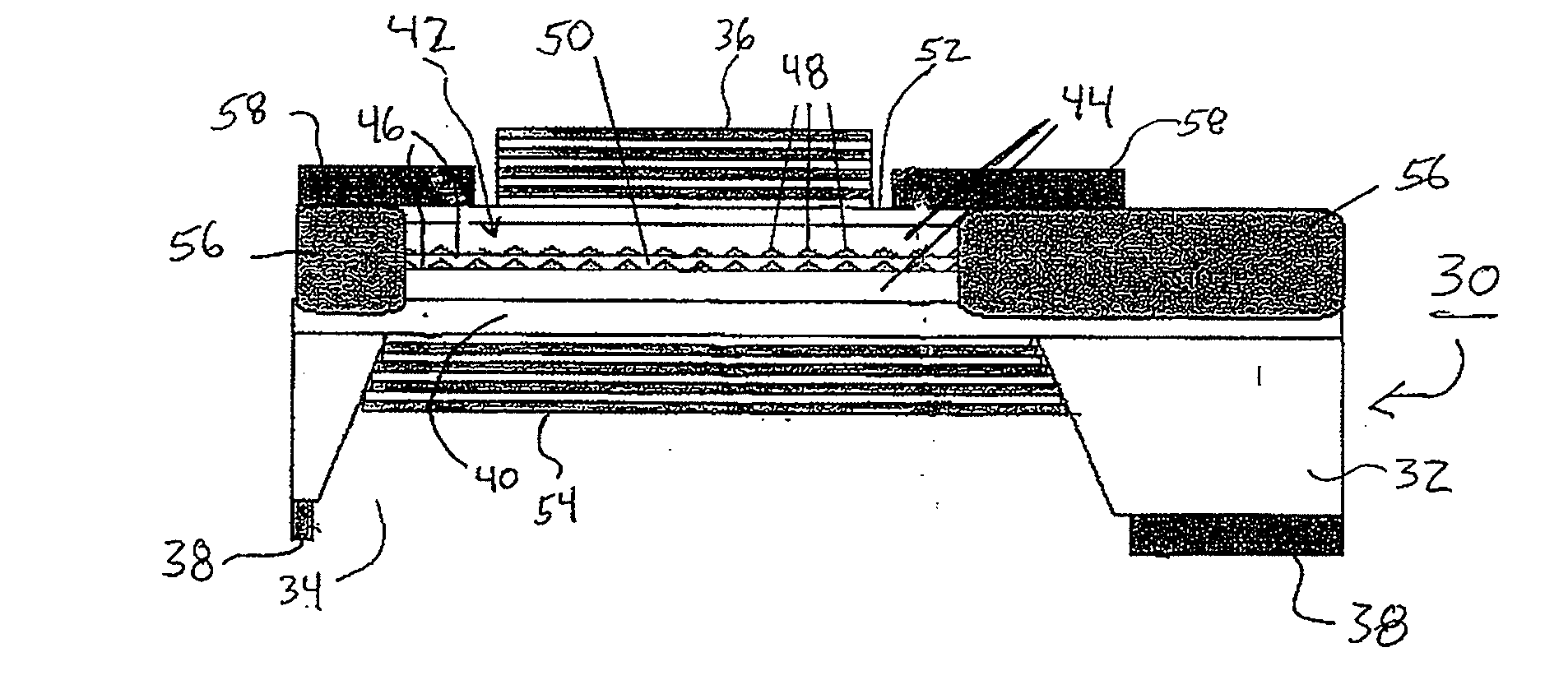
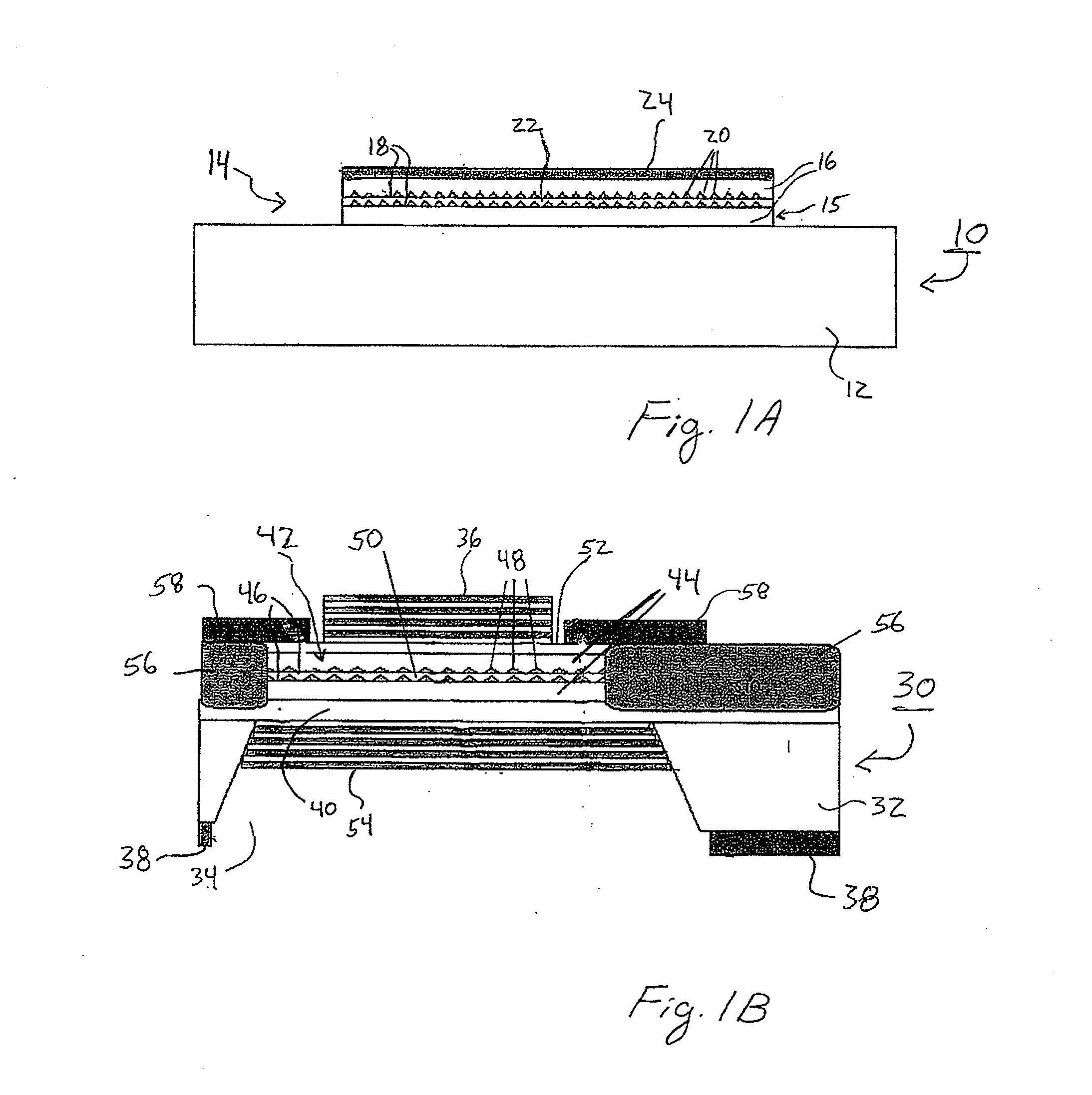
[0017]FIG. 1A illustrates a schematic representation of an edge emitting laser 10. The edge emitting laser 10 includes a p-type silicon substrate 12. An optically active region 14 is formed on the upper surface of the p-type silicon substrate 12. The optically active region 14 includes a silicon (Si) or silicon germanium (SiGe) cladding layer 16 having disposed therein one or more layers of an array 18 of quantum dots 20 formed from a compound semiconductor material. A quantum dot 20 is a cluster of atoms whose dimensions are less than the quantum mechanical wavelength of an electron or “hole.” In one preferred aspect of the invention, the quantum dots 20 are formed from semiconductor materials with a direct energy band gap. Illustrative semiconductor materials for the quantum dots 20 include InGaAs, InGaSb, PbTe, CdTe, and CdSe. In one aspect, the quantum dots20 are formed from a compound semiconductor material having a lattice mismatch with the underlying silicon buffer layer (for...


PUM


Abstract

A device having an optically active region includes a silicon substrate and a SiGe cladding layer epitaxially grown on the silicon substrate. The SiGe cladding layer includes a plurality of arrays of quantum dots separated by at least one SiGe spacing layer, the quantum dots being formed from a compound semiconductor material.

Description

RELATED APPLICATION [0001] This Application is a divisional of and claims priority to U.S. patent application Ser. No. 11 / 169,196 filed on Jun. 27, 2005. Priority is claimed under 35 U.S.C. §§120 and 121. U.S. patent application Ser. No. 11 / 169,196 is incorporated by reference as if set forth fully herein.FIELD OF THE INVENTION [0002] The field of the invention generally relates to optoelectronic devices and methods of making the same. In particular, the field of the invention relates to optoelectronic devices such as, for example, laser diodes, light emitting diodes, and photodetectors formed using quantum dots. BACKGROUND OF THE INVENTION [0003] Optoelectronic devices are becoming increasingly important to a number of industries such as, for example, the telecommunication industry. Exemplary optoelectronic-based devices include laser diodes (LD), light emitting diodes (LEDs), and photodetectors (PDs). These devices are fabricated with an optically active region made of semiconduct...

Claims


Application Information

Patent Timeline
Patent Type & Authority Applications(United States)
IPC IPC(8): H01L33/00H01L31/00
CPCB82Y10/00B82Y20/00H01L33/0066H01L33/0087H01L33/20H01S5/0207H01S5/3412H01S5/18308H01S5/18341H01S5/18369H01S5/3224H01S5/341H01S5/021Y10S977/951Y10S977/784H01L29/06
Inventor XIE, YA-HONG
Owner RGT UNIV OF CALIFORNIA
Why Eureka
Try Eureka