Electronic part module and method of making the same

a technology of electronic parts and modules, applied in the direction of printed capacitor incorporation, electrical apparatus construction details, printed circuit non-printed electric components association, etc., can solve the problems of reducing the q factor, the module cannot perform sufficiently, and the module cannot achieve sufficient size reduction, etc., to achieve the effect of increasing the manufacturing efficiency of the electronic part modul

Active Publication Date: 2008-03-06
TAIYO YUDEN KK
View PDF12 Cites 23 Cited by
  • Summary
  • Abstract
  • Description
  • Claims
  • Application Information

AI Technical Summary

Benefits of technology

[0031] The present method enables one to appropriately manufacture the electronic part module according to the first aspect of the present invention. Further, the present method, which uses a wiring substrate wafer in place of e.g. a silicon wafer common in conventional methods, is suitable for mass production of the electronic part module according to the first aspect of the present invention.
[0032] Preferably, the method further includes a step of mounting a sealing cap on each of the electronic part module formation areas on the wiring substrate wafer. The sealing step performed at the wafer level as described is preferred in view of increased manufacturing efficiency of the electronic part module.

Problems solved by technology

If an MCM-L is configured by using individual passive parts which are produced separately for surface mounting on a wiring substrate, it is sometimes impossible to accomplish sufficient size reduction of the module since surface mount type passive parts are relatively large individual chips each having their own substrate where their structures are built.
If an MCM-L is configured by using passive parts which are placed inside the wiring substrate, it is sometimes impossible for the module to perform sufficiently.
In addition, for inductors embedded in the wiring substrate, there is a problem of decreased Q factor caused by parasite capacities.
If an MCM-C is configured by using individual passive parts which are produced separately for surface mounting on a wiring substrate, it is sometimes impossible to accomplish sufficient size reduction of the module since the surface mount type passive parts are, as described above, relatively large individual chips each having their own substrate where their structures are built.
If an MCM-C is configured by using passive parts which are built inside the wiring substrate, it is sometimes impossible for the module to perform sufficiently.
In addition, for inductors embedded in the wiring substrate, there is a problem of decreased Q factor caused by parasite capacities.
If a MCM-D is configured by using individual passive parts which are produced separately for surface mounting on a wiring substrate, it is sometimes impossible to accomplish sufficient size reduction of the module since surface mount type passive parts are relatively large as described above.
If an MCM-D is configured by using passive parts which are built inside the multilayer wiring structure, it is sometimes impossible for the module to perform sufficiently.
In addition, for inductors embedded in the wiring substrate, there is a problem of decreased Q factor caused by parasite capacities.

Method used


Image

  • Electronic part module and method of making the same
  • Electronic part module and method of making the same
  • Electronic part module and method of making the same

Examples


first embodiment

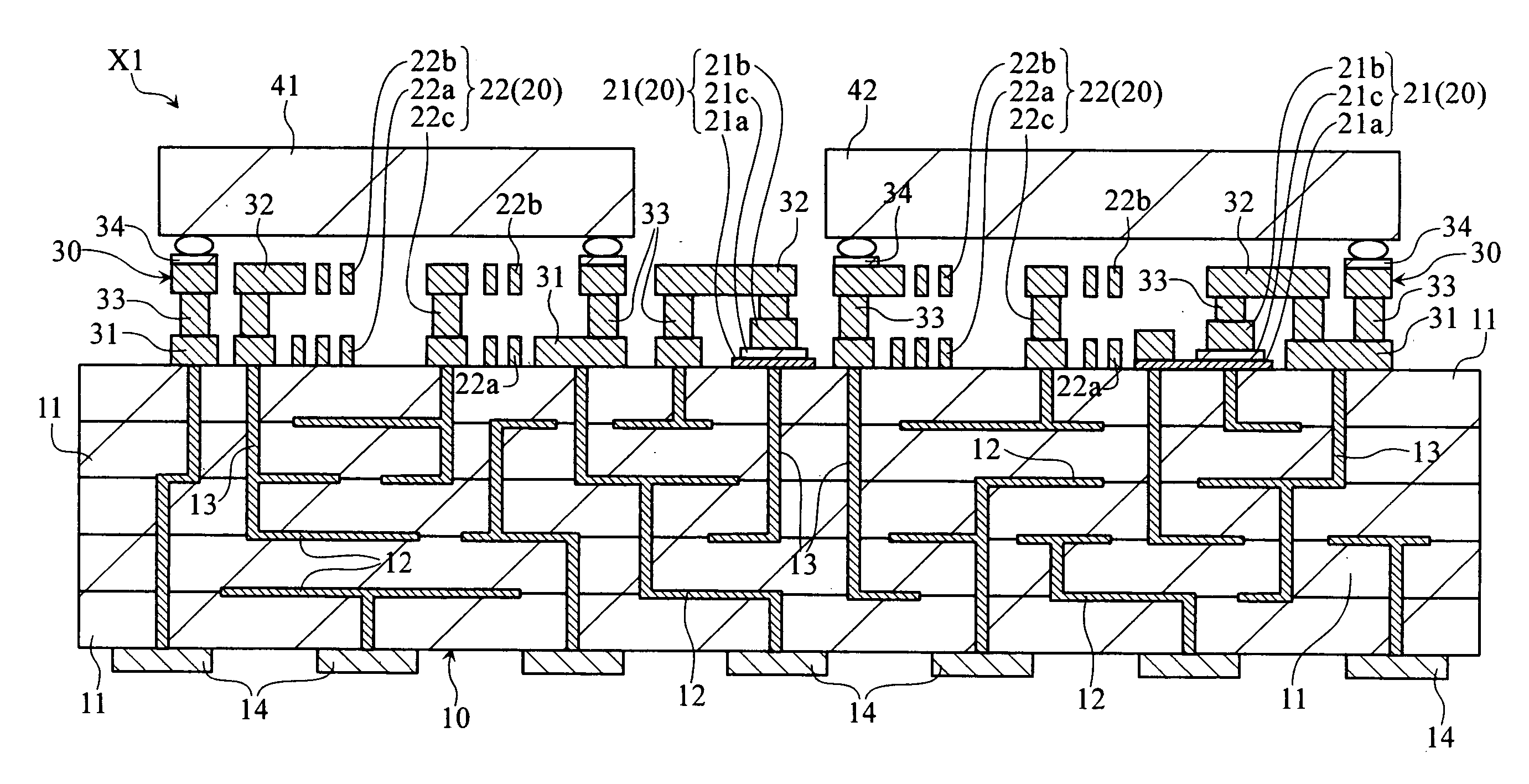
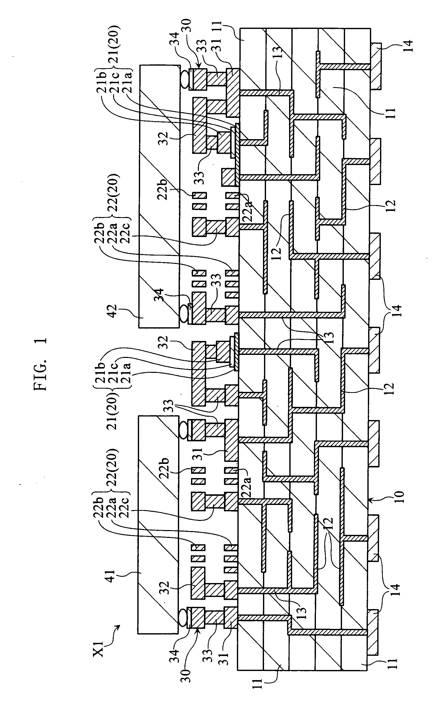
[0053]FIG. 1 is a sectional view of an electronic part module X1 according to the present invention. The electronic part module X1 includes a wiring substrate 10, a passive device group 20, three-dimensional wiring 30, and device chips 41, 42.

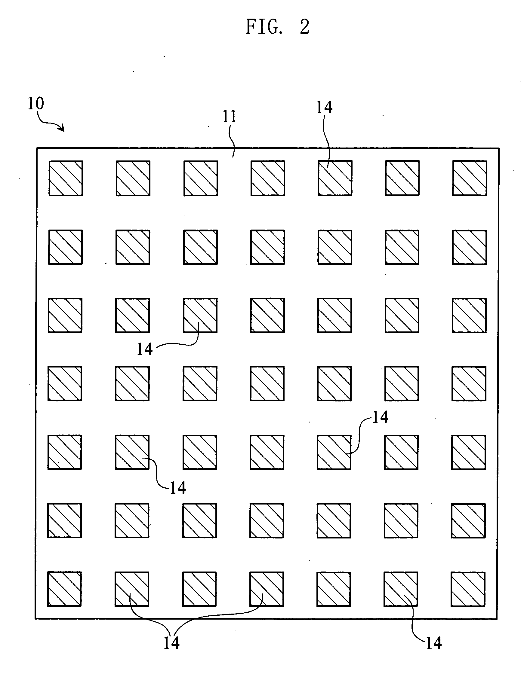
[0054] The wiring substrate 10 is a multilayer ceramic wiring substrate, and includes insulating layers 11, wiring patterns 12, vias 13 and external connection pads 14. Each insulating layer 11 is provided by a ceramic layer of e.g. Al2O3. Each wiring pattern 12 is formed of Cu, Ag, W or Mo for example, into a predetermined pattern between insulating layers 11. Each via 13 is formed of Cu, Ag, W or Mo, penetrates insulating layers 11 and makes a connection with a wiring pattern(s) 12. Some of the vias 13 provide connection between wiring patterns 12. Each pad 14 is formed of Cu for example, on one surface of the wiring substrate 10. The pads 14 may be made of Ni coated with a film of Au. The pads 14 are arrayed as in FIG. 2, on a surface of the...

second embodiment

[0089]FIG. 12 is a sectional view of an electronic part module X2 according to the present invention. The electronic part module X2 differs from the electronic part module X1 in that it further includes a sealing cap 51. The sealing cap 51 is made of a metal material or a ceramic material for example. The sealing cap 51 provides air-tight sealing over the passive device group 20, the three-dimensional wiring 30 and the device chips 41, 42 on the wiring substrate 10.

[0090] The electronic part module X2 can be manufactured by the same method as for the electronic part module X1, with an additional step (sealing step) of mounting the sealing cap 51 onto the wiring substrate wafer 10′ after the device chip mounting step described with reference to FIG. 9(c) and before the dicing step. In the sealing step, the sealing cap 51 is bonded to the wiring substrate wafer 10′ (the wiring substrate 10) via a sealing material 52. The sealing material 52 is provided by solder, glass frit or resin m...

third embodiment

[0092]FIG. 13 is a sectional view of an electronic part module X3 according to the present invention. The electronic part module X3 differs from the electronic part module X1 in that it includes a device chip 43 in place of the device chips 41, 42, and further includes a peripheral wall 53. The device chip 43 is a one-chip version of a plurality of device chips (such as the device chips 41, 42), and is mounted so as to cover the passive device group 20 and the three-dimensional wiring 30 entirely on the wiring substrate 10. The peripheral wall 53 is formed to surround the perimeter of the passive device group 20 on the wiring substrate 10. The device chip 43 is fixed to the wiring substrate 10 via the three-dimensional wiring 30 and via the peripheral wall 53 as well. The peripheral wall 53 is made of a metal material for example. The device chip 43 and the peripheral wall 53 as described provide air-tight sealing for the passive device group 20 and the three-dimensional wiring 30 o...


PUM

PropertyMeasurementUnit
thicknessaaaaaaaaaa
thicknessaaaaaaaaaa
thicknessaaaaaaaaaa

Abstract

An electronic part module includes a wiring substrate, a passive device group of passive devices formed on the wiring substrate, and device chips mounted on the wiring substrate. Such an electronic part module is made in the following manner. First, a wiring substrate wafer is made, to include a plurality of electronic part module formation areas. Then, a plurality of passive devices are formed in each of the electronic part module formation areas on the wiring substrate wafer. Then, the device chips are formed on each of the electronic part module formation areas on the wiring substrate wafer. Finally, the wiring substrate wafer is divided.

Description

BACKGROUND OF THE INVENTION [0001] 1. Field of the Invention [0002] The present invention relates to an electronic part module, in particular an electronic module which contain a plurality of device chips and a plurality of passive parts as their constituent elements. The present invention also relates to a manufacturing method of the electronic part modules. [0003] 2. Description of the Related Art [0004] Our information society is dependent upon a variety of information processing equipment including mainframe computers, personal computers and mobile communication terminals. In all of these fields, efforts are being made for higher processing speed, smaller size of equipment, increased versatility, reduced power consumption, and so on. All of these improvements are mainly dependent upon improved level of circuit integrity and performance (higher speed, advanced functionality, etc.) of numerous semiconductor devices incorporated in the equipment and apparatuses. Multi-chip module (...

Claims


Application Information

Patent Timeline
Patent Type & Authority Applications(United States)
IPC IPC(8): H05K1/16H05K3/00H05K7/02
CPCH01L23/5389Y10T29/49124H01L23/645H01L25/16H01L2224/16H01L2924/01078H01L2924/01079H01L2924/09701H01L2924/16152H01L2924/19015H05K1/162H05K1/165H05K3/0052H05K3/4685H05K2201/0394H05K2201/10674H05K2203/0574H05K2203/308H01L23/642H01L2924/00014H01L2924/00011H01L2224/0401H05K1/18H05K3/34H01L23/12
Inventor MI, XIAOYUMATSUMOTO, TSUYOSHIUEDA, SATOSHI
Owner TAIYO YUDEN KK
Why Eureka
Try Eureka