Method of manufacturing a semiconductor device

a manufacturing method and semiconductor technology, applied in semiconductor/solid-state device manufacturing, basic electric elements, electric devices, etc., can solve the problems of inability to remove the deposit using cleaning gas, low production efficiency, and high so as to improve the productivity of the semiconductor device, reduce the cost of organic materials, and reduce the effect of etching depth

Inactive Publication Date: 2008-03-06
RENESAS ELECTRONICS CORP
View PDF22 Cites 5 Cited by
  • Summary
  • Abstract
  • Description
  • Claims
  • Application Information

AI Technical Summary

Benefits of technology

[0010]Even if the cleaning step is provided as described in the above patent document, the deposit adhered to the inner wall of the chamber can be not completely removed. Thereby, there has been a case in which, when a plurality of wafers are continuously processed in one and the same chamber, etching characteristics are influenced by deposits at an etching step for to be processed later. Accordingly, there have been some problems in which there are caused variations in etching depths of via holes, interconnect trenches, and the like between wafers and within a same wafer to increase interconnect resistances, contact resistances, and the like.
[0013]As shown in FIG. 4B, the another wafer 42 is mounted in the chamber of the etching equipment 32 in a similar manner to that of FIG. 4A. Then, a predetermined voltage is applied to between the upper electrode 34 and the lower electrode 36, and a target film is etched, using etching gas as plasma 38. An SiOCH film is used as a target film, and CF4 / N2 (or CH2F2 / CF4 / Ar / O2) is adopted as etching gas. In the above etching step, a deposit 40, which has adhered to the inner wall of the chamber 32, is re-dissociated, and a nitrogen atom in the deposit 40 (or a hydrogen atom) is mixed with the etching gas. Thereby, it may be considered that nitrogen gas concentration (or hydrogen gas concentration) in the vicinity of the inner wall of the chamber 32 is increased to improve an etching grade on the outer edge of the wafer 42.
[0018]Thereby, another same kind of substrate to be processed is carried into the etching equipment after completing the etching step of the substrate to be processed, and the same etching step is executed, and the productivity of the semiconductor device may be improved. That is, as the amount of nitrogen atoms and that of hydrogen atoms, which are included in deposits, are reduced at the etching step, influences by the nitrogen atoms and the hydrogen atoms may be suppressed when the second insulating film in the second and subsequent substrates to be processed are etched. Variations in etching depths of via holes, interconnect trenches, and the like within a same wafer and between wafers can be suppressed, and the productivity of the semiconductor device may be improved.
[0019]According to the present invention, influences of deposits, which have adhered to the inner wall of the chamber, may be removed at the etching step. Thereby, there is provided the method of manufacturing a semiconductor device by which variations in etching depths of via holes, interconnect trenches, and the like between wafers and within a same wafer can be suppressed, and an increase in interconnect resistances, that in contact resistances, and the like can be suppressed.

Problems solved by technology

However, the organic material is generally expensive.
Accordingly, there have been some problems in which there are caused variations in etching depths of via holes, interconnect trenches, and the like between wafers and within a same wafer to increase interconnect resistances, contact resistances, and the like.
Thereby, there have been some problems in which there are caused variations in etching depths of via holes, interconnect trenches, and the like between wafers and within a same wafer.
Accordingly, the method removing the deposit by using the cleaning gas has not been adopted.

Method used


Image

  • Method of manufacturing a semiconductor device
  • Method of manufacturing a semiconductor device
  • Method of manufacturing a semiconductor device

Examples


example

[0079]Etching was performed according to the all-in-one etching method described in FIGS. 1A to 3B under the following conditions according to the following testing method.

[0080]Step (1): Only an Si substrate was mounted in a chamber of an etching equipment, and plasma generation of etching gas described in FIG. 5 was performed.

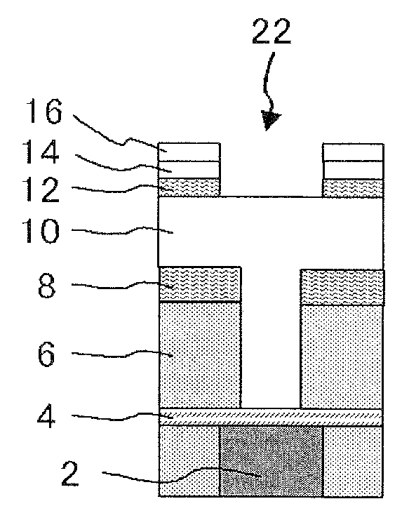
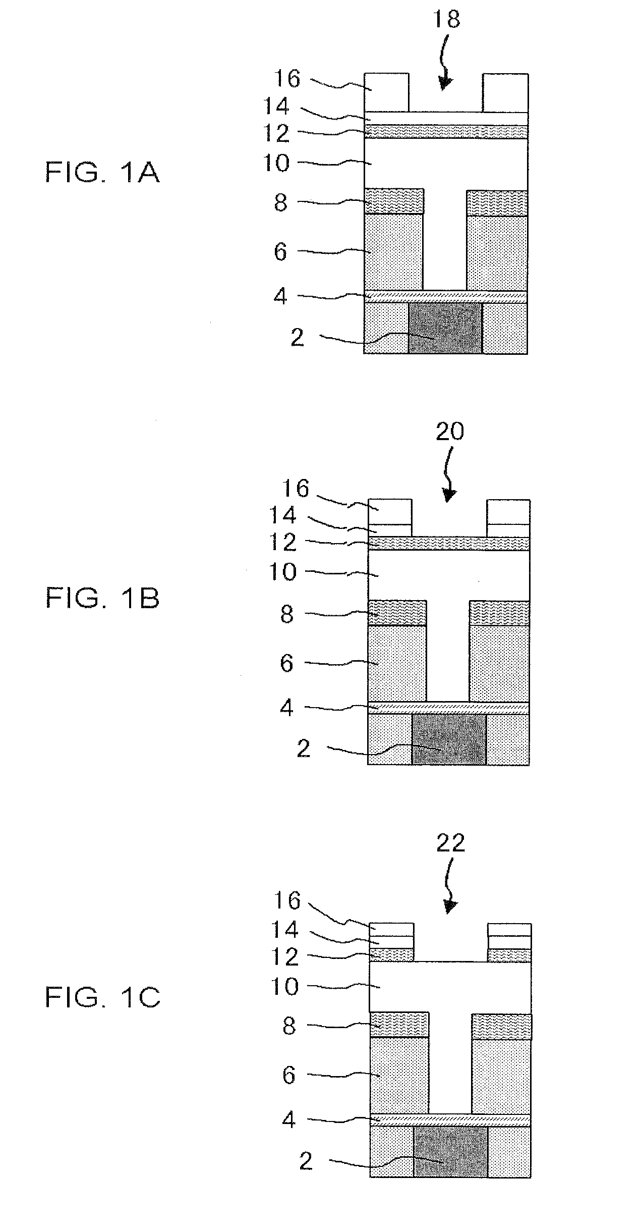
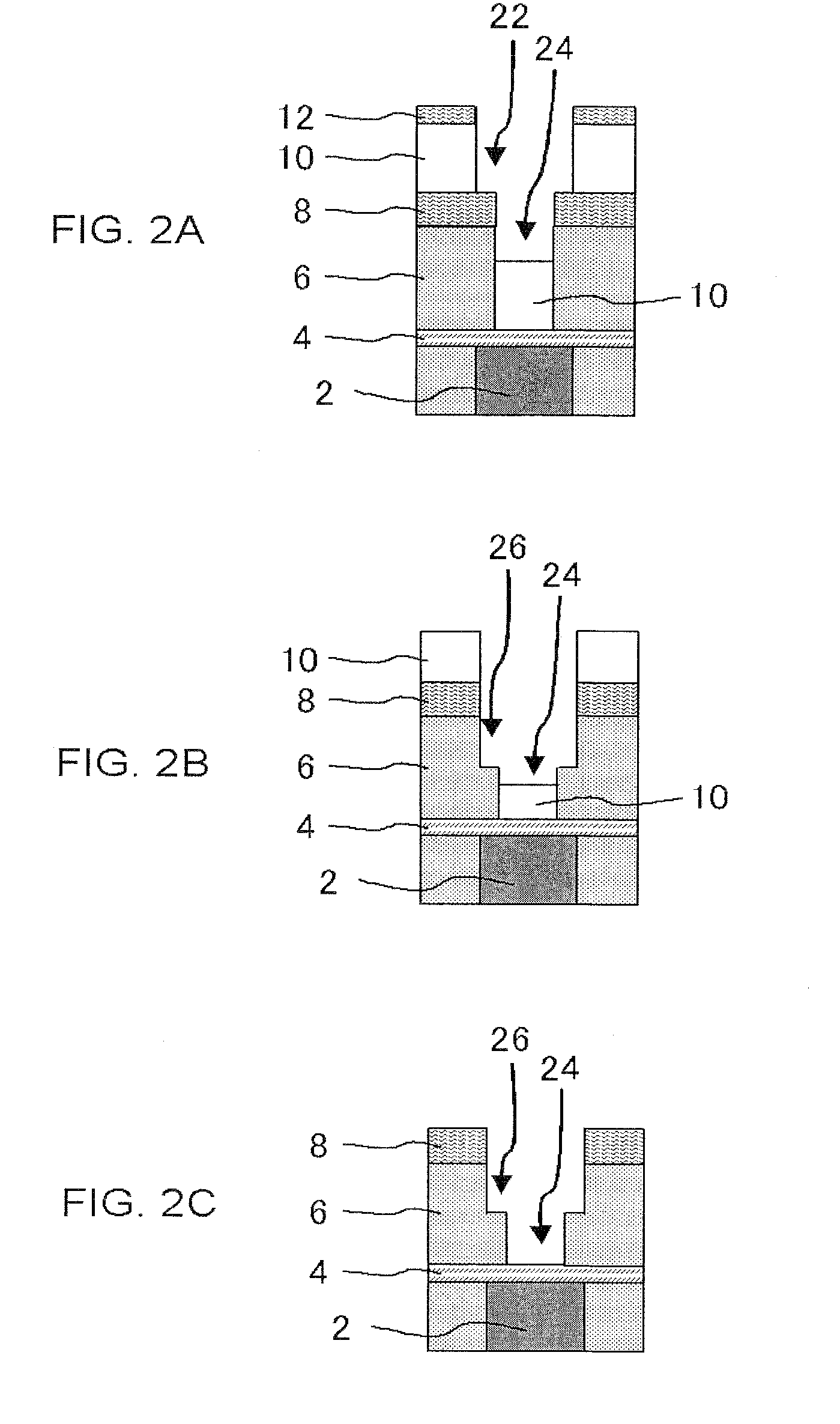
[0081]Step (2): The Si substrate used at the above-described step (1) was taken out, and the substrate with a stacked film was etched under the following conditions according to the etching steps described in FIGS. 1A to 3B. Steps to an ashing step for a resist film 10 were completed, and there was confirmed a difference in etching depth for an interlayer film 6 (SiOCH film) between in the center portion (denoted by “Cntr” in FIG. 5) and in the outer edge (at a position 4 mm inward from the outside edge (denoted by “4 mm” in FIG. 5)) of the wafer. Here, the tests were conducted in a portion in which a via hole like the via hole shown in FIG. 1A was not provid...


PUM


Abstract

Method of manufacturing a semiconductor device including arranging a substrate having a stacked film containing a first insulating film and a second insulating film formed thereon in an etching equipment, etching the first and second insulating film in the etching equipment, the first insulating film comprised of a nitrogen-containing film, and the second insulating film comprised of one or more kinds of films selected from a group consisting of an SiOCH film, an SiO2 film, a methyl silsesquioxane film, a hydrogen silsesquioxane film and a methyl hydrogen silsesquioxane film, while using as etching gas (a) gas including fluorocarbon represented by CxFy (x: an integer from 1 to 6, and y: an integer from 4 to 12), or (b) mixed gas of the fluorocarbon and one or more kinds of gas selected from a group consisting of O2, Ar and CO.

Description

[0001]This application is based on Japanese patent application Nos. 2006-233156 and 2007-159950, the contents of which are incorporated hereinto by reference.BACKGROUND[0002]1. Technical Field[0003]The present invention relates to a method of manufacturing a semiconductor device, including steps at which a stacked film is etched in one and the same etching equipment.[0004]2. Related Art[0005]Recently, a processing method using a so-called all-in-one etching method in which a plurality of etching steps are performed in one and the same equipment has become mainstream in order to suppress the manufacturing cost of a semiconductor device (refer to Japanese Laid-Open Patent Publication Nos. 2003-45964, 2003-309107, and 2005-353698).[0006]Moreover, Japanese Laid-Open Patent Publication No. 2003-45964 has disclosed an example in which a dual damascene structure is formed according to the all-in-one etching technique, using an organic material as an interlayer insulating film. However, the...

Claims


Application Information

Patent Timeline
Patent Type & Authority Applications(United States)
IPC IPC(8): H01L21/302
CPCH01L21/31116H01L21/76808H01L21/31138
Inventor NANBU, HIDETAKA
Owner RENESAS ELECTRONICS CORP
Why Eureka
Try Eureka