
Method and apparatus for fast identification of high stress regions in integrated circuit structure

Active Publication Date: 2008-03-13
SYNOPSYS INC
View PDF3 Cites 24 Cited by
  • Summary
  • Abstract
  • Description
  • Claims
  • Application Information

AI Technical Summary

Benefits of technology

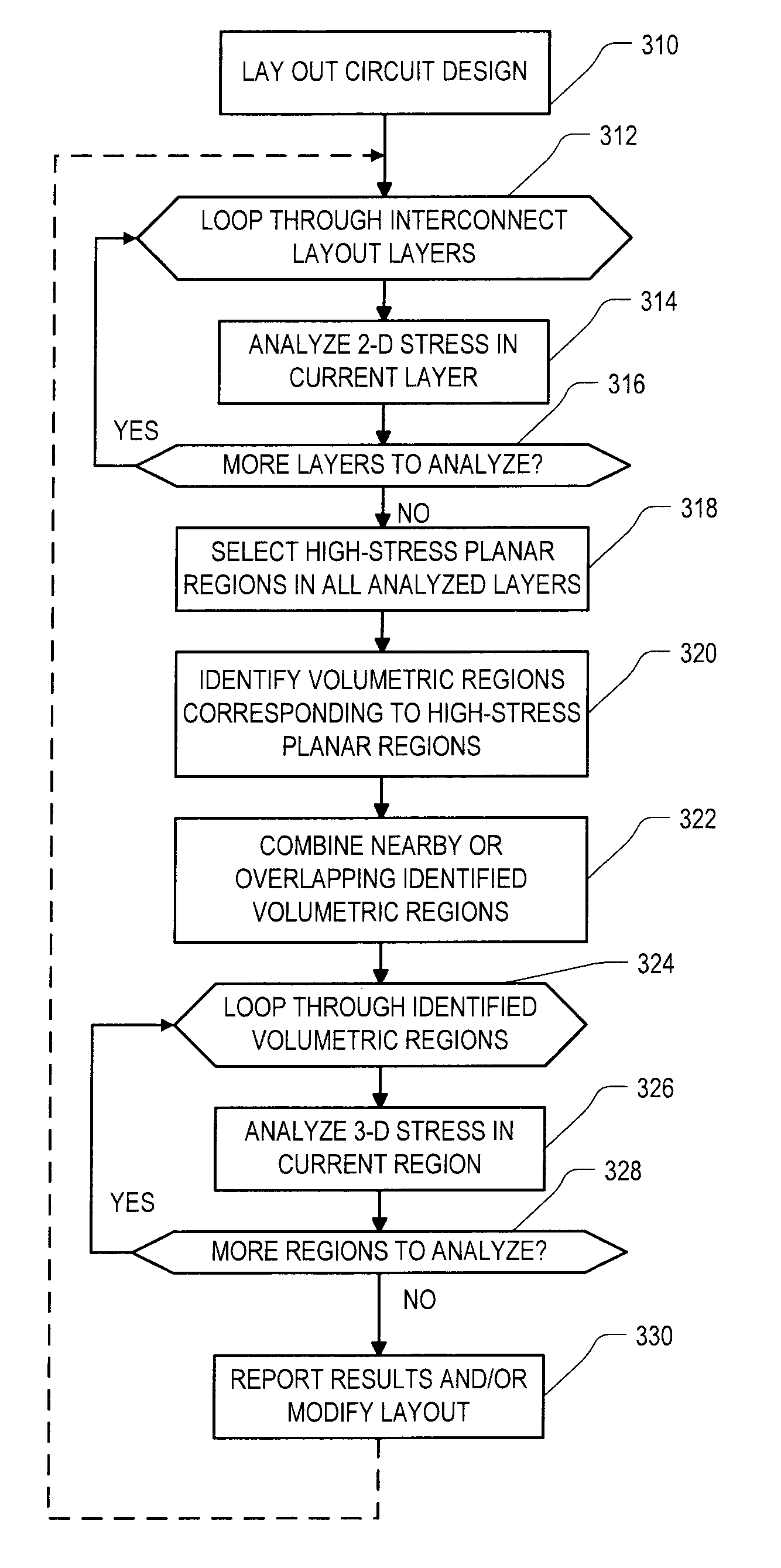
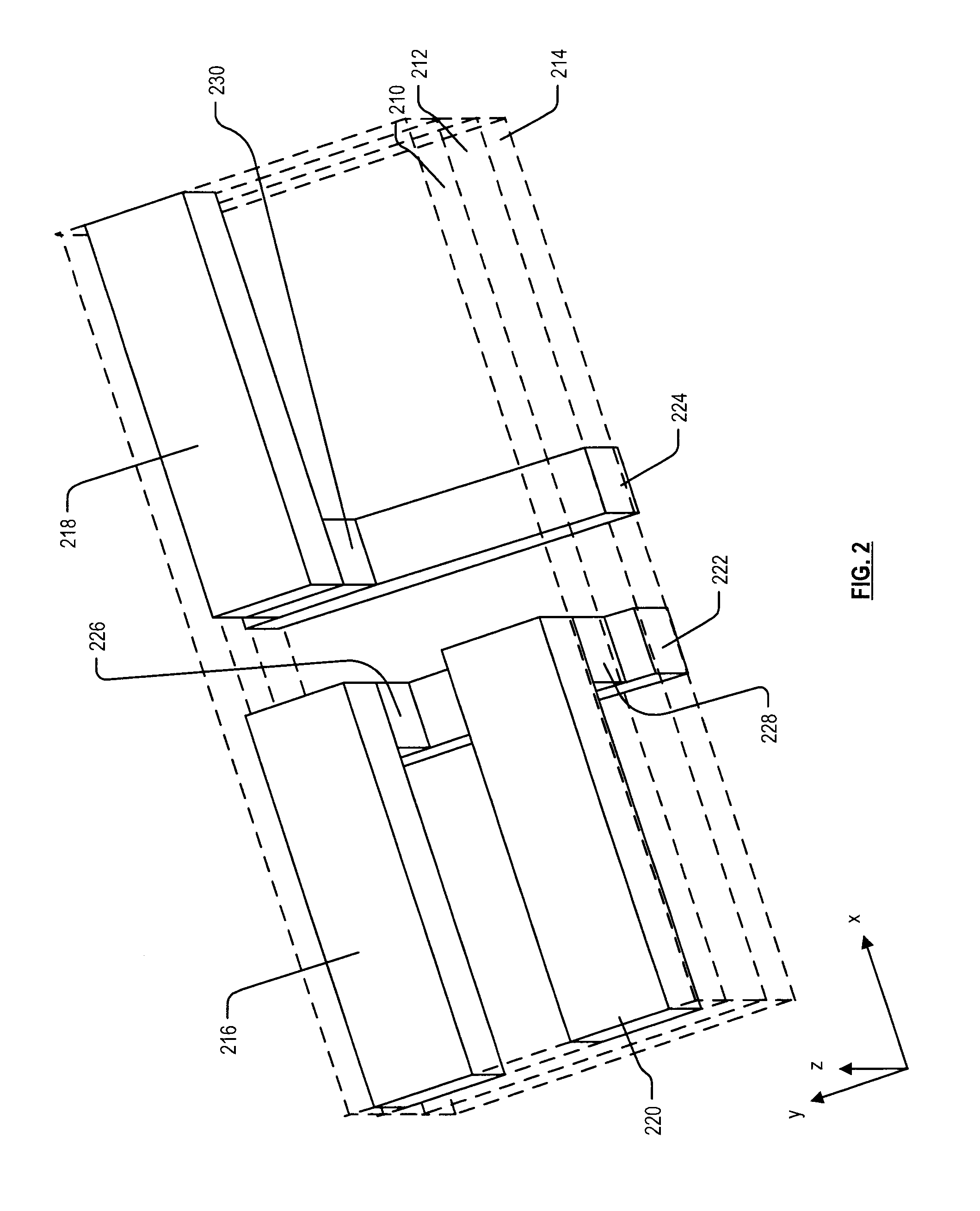
[0005]It has now been recognized that because of the specific geometry and material composition of logic based interconnects, there is a strong correlation between high stress distributions on a 2-dimensional layout plane and that in the 3-dimensional interconnect structure defined by the 2-dimensional layout. In addition, it has been recognized that the analysis window for a 2-dimensional analysis can be quite small around the structures. Based on these insights and others a high performance stress analyzer can be developed which can allow a large design layout to be analyzed. Roughly described, the analyzer first scans layout layers with a 2-dimensional stress analyzer, to predict regions of high 2-dimensional stress. 3-dimensional structures corresponding to those 2-dimensional regions can then be further analyzed locally with a 3-dimensional stress simulator for more accurate volume stress distributions. The 2-dimensional analysis is much simpler and much quicker than a 3-dimensional analysis, and can greatly reduce the number and size of volumetric regions for 3-dimensional analysis. As a result, it is now practical to analyze the layout for an entire chip for high stress regions, and to do so much more quickly than was previously required to perform a 3-dimensional analysis on only a small part of the chip layout.

Problems solved by technology

Material property mismatch between the interconnect material and the dielectric material often introduces thermal mismatch stress in the interconnect structures.
High stress in localized regions, such as the region between two line ends or at vias, can lead to yield or field failures from dielectric cracking, interface de-bonding, or metal voiding.
This problem has increased in significance with the adoption of low-k dielectric materials, which typically have lower mechanical strength than the more traditional dielectric materials, although it can arise with the traditional materials as well.
But since stress failure due to inter-layer material property mismatches is inherently a 3-dimensional problem, 3-dimensional stress analysis of volumetric (3-dimensional) regions of the device was typically required.
Such analysis was typically performed using a 3-dimensional finite element analysis, which is exceedingly time consuming.
It is prohibitive to analyze large layouts using this method.
As a result, the design and technology community is not currently able to fully analyze large layouts for mechanical stress performance based on layout data.
In addition, it can be seen from the above that stress-related integrated circuit reliability issues often arise from structures that extend deeply into the device, spanning multiple layers.

Method used


Image

  • Method and apparatus for fast identification of high stress regions in integrated circuit structure
  • Method and apparatus for fast identification of high stress regions in integrated circuit structure
  • Method and apparatus for fast identification of high stress regions in integrated circuit structure

Examples


Embodiment Construction

[0019]The following description is presented to enable any person skilled in the art to make and use the invention, and is provided in the context of a particular application and its requirements. Various modifications to the disclosed embodiments will be readily apparent to those skilled in the art, and the general principles defined herein may be applied to other embodiments and applications without departing from the spirit and scope of the present invention. Thus, the present invention is not intended to be limited to the embodiments shown, but is to be accorded the widest scope consistent with the principles and features disclosed herein.

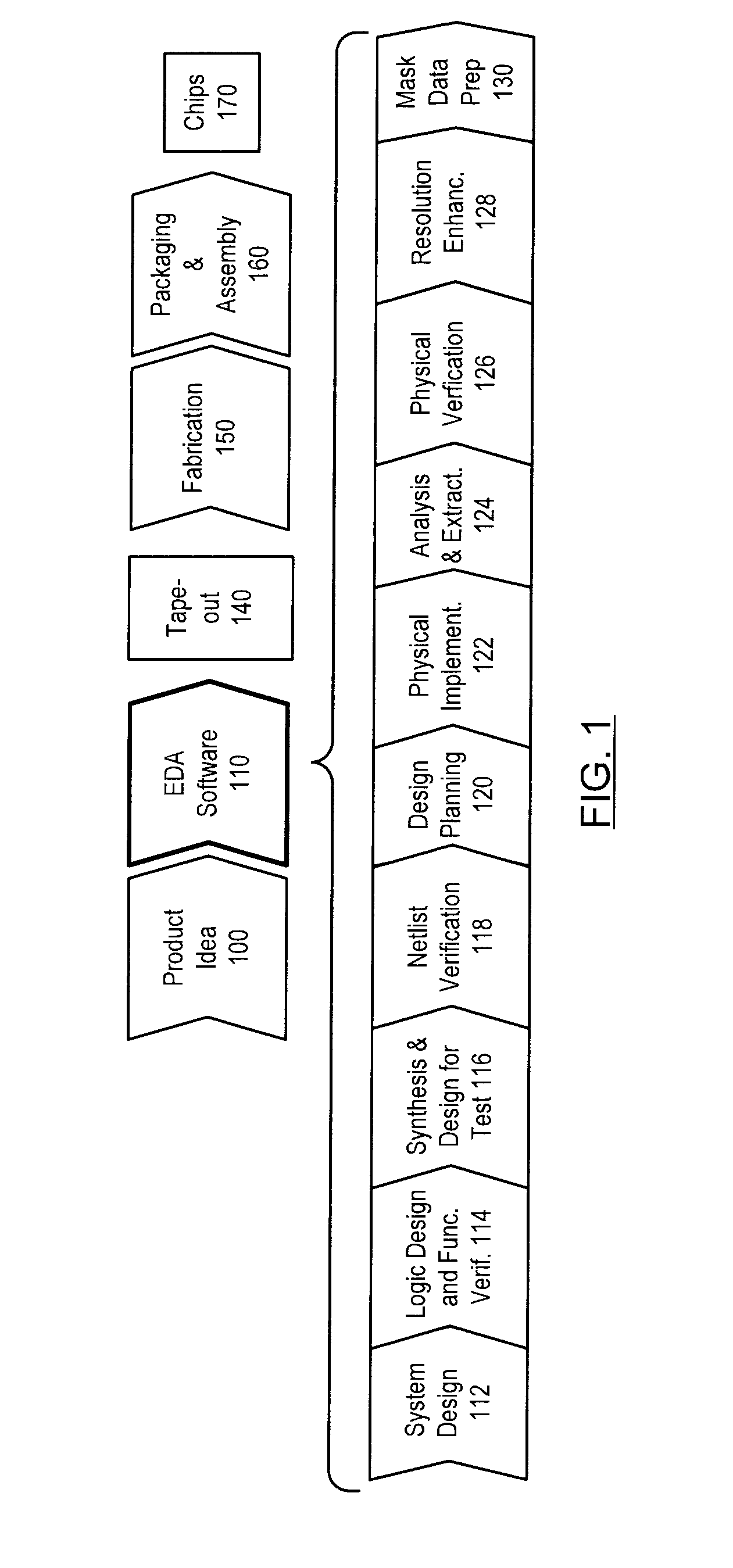
[0020]FIG. 1 shows a simplified representation of an illustrative digital integrated circuit design flow. At a high level, the process starts with the product idea (step 100) and is realized in an EDA (Electronic Design Automation) software design process (step 110). When the design is finalized, it can be taped-out (step 140). After tape out, ...


PUM


Abstract

Roughly described, high-stress volumetric regions of an integrated circuit structure are predicted by first scanning one or more layout layers to identify planar regions of high 2-dimensional stress, and then performing the much more expensive 3-dimensional stress analysis only on volumetric regions corresponding to those planar regions that were found to have high 2-dimensional stress. A windowing method can be used for the 2-dimensional scan, optionally with an overlap region extending slightly into adjacent windows. Very narrow features arising at the edges of an analysis window can be relocated to the edge of the analysis window in order to avoid numerical artifacts.

Description

BACKGROUND AND SUMMARY OF THE INVENTION[0001]The present invention relates to stress analysis of integrated circuits, and more particularly, to fast techniques for identifying high-stress regions.[0002]A typical integrated circuit device includes a number of interconnect layers alternating with dielectric layers, all superposing a silicon substrate. Many of the dielectric layers are also referred to as via layers, because they include holes, or vias, in specific locations to allow the formation of conductive material passing from one interconnect layer to another, or from one interconnect layer to a desired point on the substrate. The material in the via connects above to a conducting trace and below to either another conducting trace or to the substrate.[0003]Material property mismatch between the interconnect material and the dielectric material often introduces thermal mismatch stress in the interconnect structures. Stresses can also arise from other sources such as intrinsic / gra...

Claims


Application Information

Patent Timeline
IPC IPC(8): G06F17/50
CPCG06F17/5081G06F17/5018G06F30/398G06F30/23
Inventor XU, XIAOPENGPRAMANIK, DIPANKAR
Owner SYNOPSYS INC
Learn More