

Electron beam apparatus and an aberration correction optical apparatus
- Summary
- Abstract
- Description
- Claims
- Application Information
AI Technical Summary
Benefits of technology
Problems solved by technology
Method used
Image

Examples
second embodiment
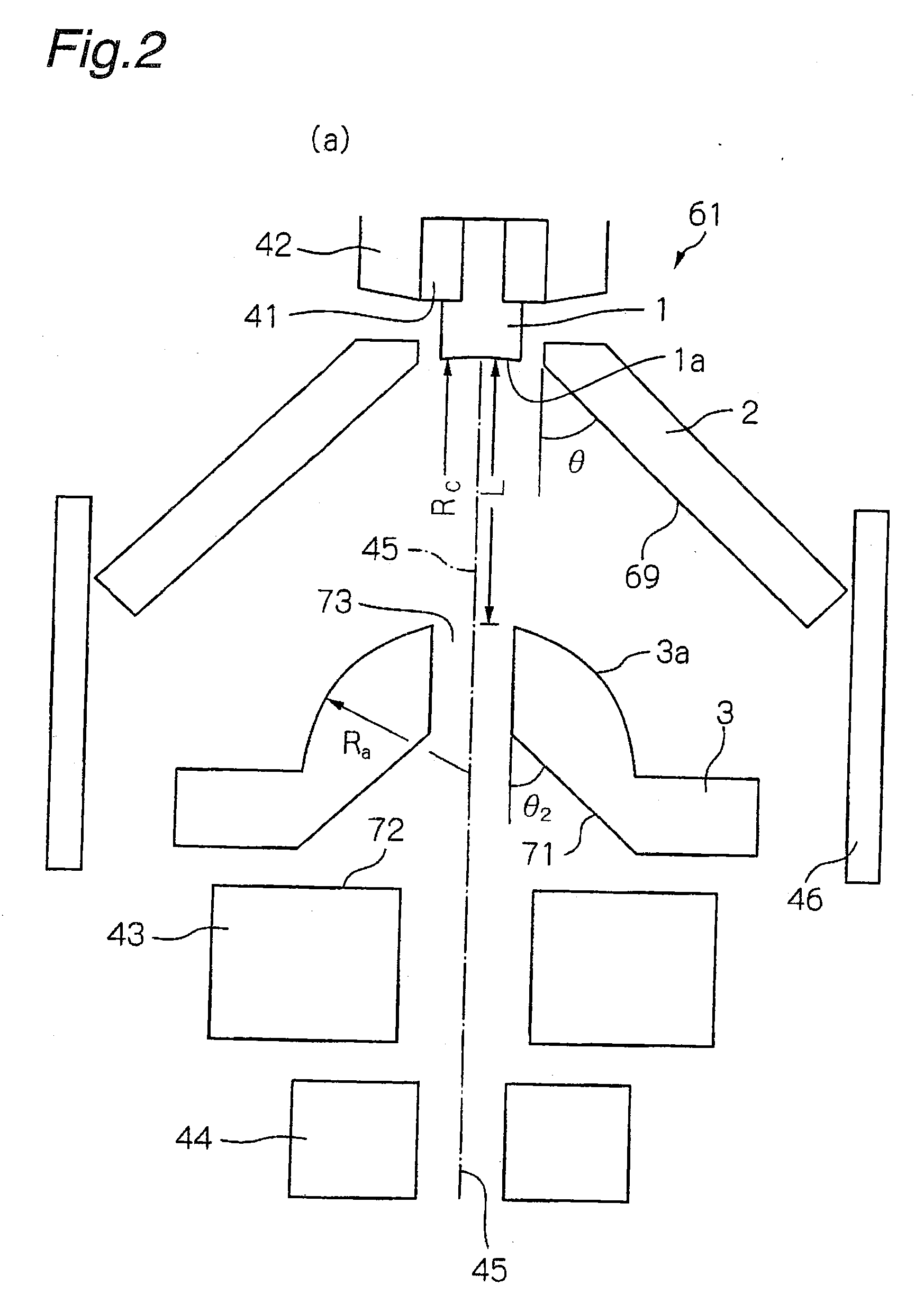
[0067] the present invention is configured such that the relationship among the distance L along the optical axis between the curved surface (the first sphere) 1a defining the electron emission surface of the cathode and the convex surface (the second sphere) 3a of the drawing electrode, the radius of curvature, Rc, of the curved surface (the first sphere) 1a and the radius of curvature, Ra, of the convex surface (the second sphere) 3a satisfies an inequity defined by:
2Rc<L+Ra (2)
third embodiment
[0068] the present invention is configured such that the relationship among the distance L along the optical axis between the curved surface (the first sphere) 1a defining the electron emission surface of the cathode and the convex surface (the second sphere) 3a of the drawing electrode, the radius of curvature, Rc, of the curved surface (the first sphere) 1a and the radius of curvature, Ra, of the convex surface (the second sphere) 3a satisfies an inequity defined by:
2Ra<Rc−L (3)
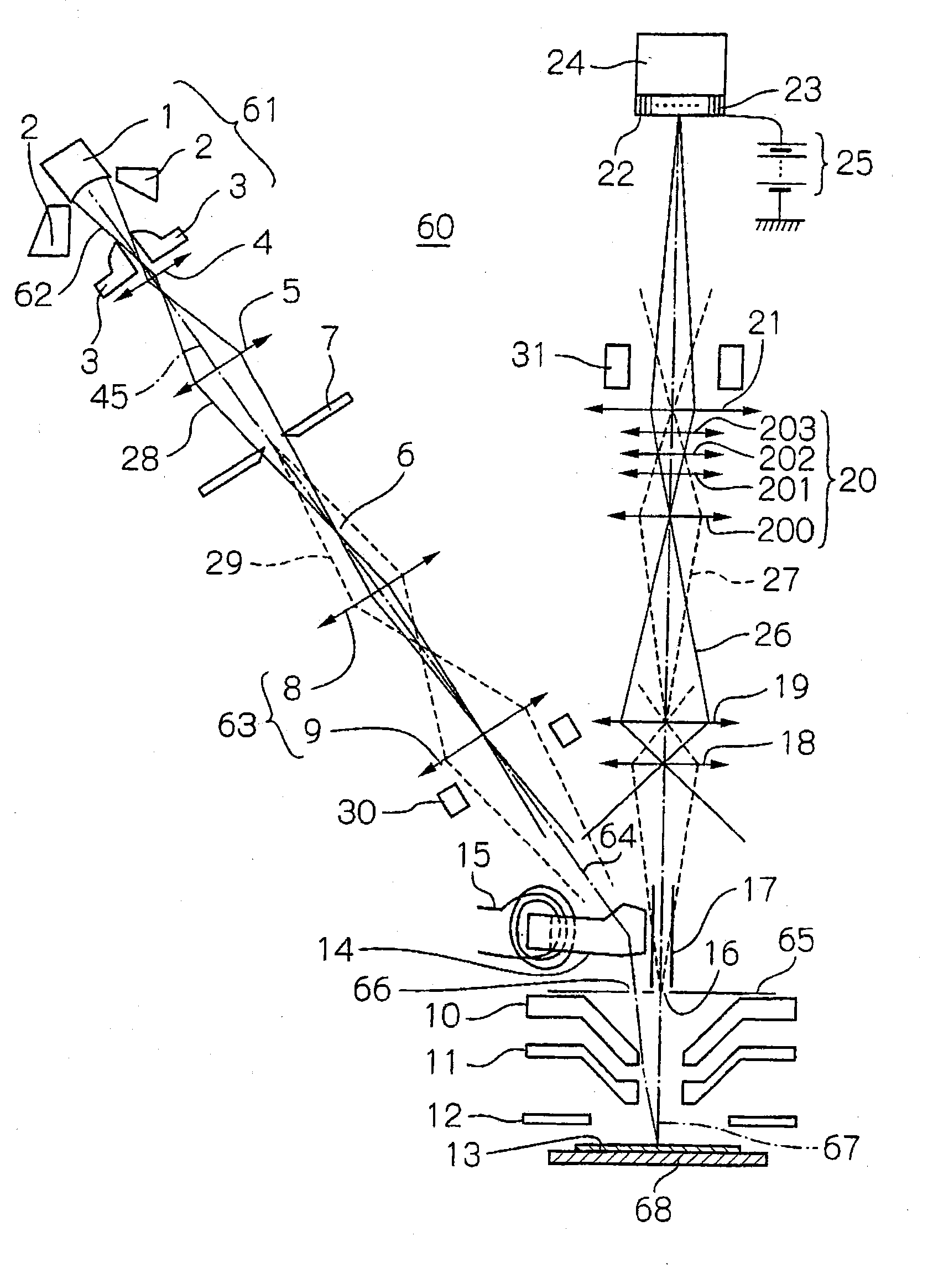
[0069] For the Pierce type electron gun, which satisfies an equation defined by L=Rc−Ra, the curvature surface (the first sphere) 1a and the curvature surface (the second sphere) 3a represent concentric spheres. As obviously seen from the comparison to that, the cathode-anode distance L defined by the above inequity (1) is longer than a difference between the radii of concentric spheres. FIG. 7 shows a graphical representation of a beam property from a simulation taking the Rc=5 mm, Ra=2 mm and L=4 mm ...
first embodiment
[0083] This allows the G trajectory to have a more ideal double symmetry over the present invention. Further in this configuration, since a deflector can be placed in the intermediate image-formation plane, the load to the power supply can be reduced preferably to the first example of the present invention.
[0084] It is to be noted also with this embodiment that each of the unipotential lenses 103a may be constructed in the multi-polar structure by overlapping dipolar or quadrupolar fields to serve for providing axial adjustment and for compensating for a gap resulting from a magnification scale. Although, instead of the unipotential lens 103a, a rotationally symmetric lens or an electromagnetic lens having the multi-polar structure may be employed, the electrostatic type may be more preferably employed from the consideration of the rotational effect on the image. As is the case with the previous embodiment, none of the unipotential lenses are necessarily rotationally symmetric lense...
PUM
 Abstract
Description
Claims
Application Information