Field-effect transistor and method for manufacturing the same

Inactive Publication Date: 2008-03-20
CANON KK
View PDF0 Cites 117 Cited by
  • Summary
  • Abstract
  • Description
  • Claims
  • Application Information

AI Technical Summary

Benefits of technology

[0060]The field-effect transistors illustrated in FIGS. 1A and 1B include the substrate 10, the source electrode 11, the drain electrode 12, the oxide semiconductor layer 13, the gate insulating layer 14, and the gate electrode 15. The characteristics of each component are described above.
[0061]The phrase “the concentration of hydrogen or deuterium in the regions in the oxide semiconductor layer 13 in contact with the source electrode 11 and the drain electrode 12”, as used herein, means the concentration of hydrogen or deuterium in the oxide semiconductor layer 13 in the vicinities of the source electrode 11 and the drain electrode 12.
[0062]The concentration of hydrogen or deuterium in the regions in the oxide semiconductor layer 13 in contact with the source electrode 11 and the drain electrode 12 is higher than the average concentration of hydrogen or deuterium in the oxide semiconductor layer 13. Thus, the higher concentration of hydrogen or deuterium in the regions in the oxide semiconductor layer 13 in contact with the source electrode 11 and the drain electrode 12 reduces the parasitic resistance.
[0063]The concentration of hydrogen or deuterium in the regions in the oxide semiconductor layer 13 in contact with the source electrode 11 and the drain electrode 12 and the average concentration of hydrogen or deuterium in the oxide semiconductor layer 13 may be determined from the composition distribution of the oxide semiconductor layer 13 in the depth direction measured by SIMS. The regions in the oxide semiconductor layer 13 in contact with the source electrode 11 and the drain electrode 12 are sufficient for the regions in which hydrogen or deuterium diffuses. However, if the semiconducting properties are not adversely affected, hydrogen or deuterium may be caused to diffuse toward the gate insulating layer 1

Problems solved by technology

However, a ZnO-based compound cannot form a stable amorphous phase at room temperature, but forms a polycrysta

Method used


Image

  • Field-effect transistor and method for manufacturing the same
  • Field-effect transistor and method for manufacturing the same
  • Field-effect transistor and method for manufacturing the same

Examples


example 1

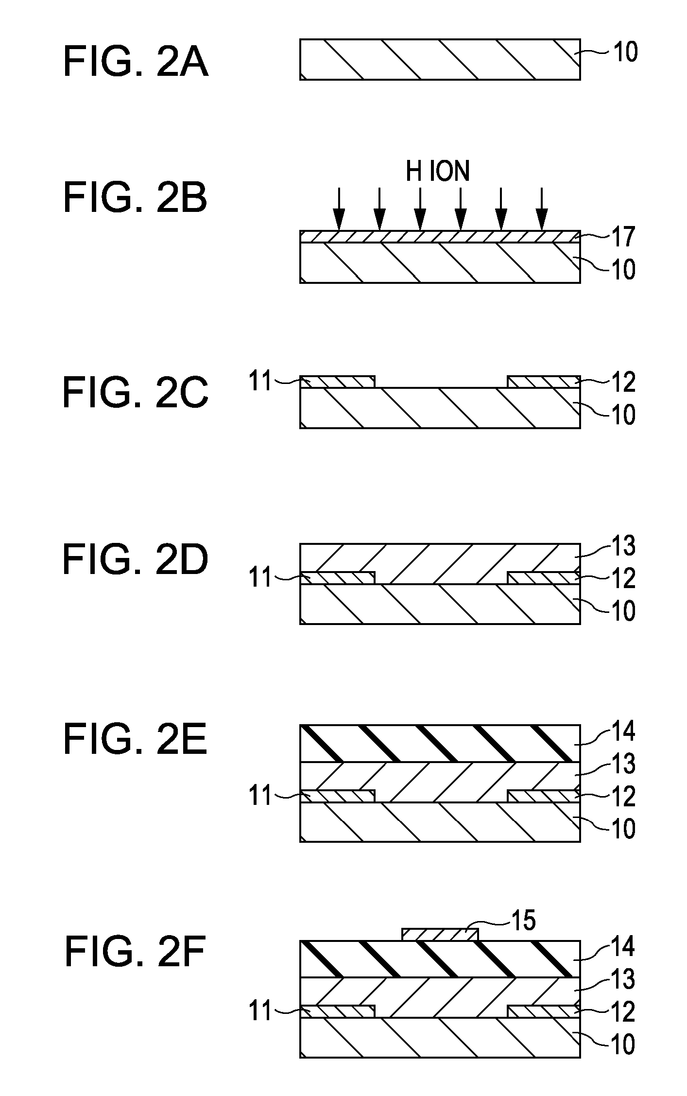
[0072]FIGS. 2A-2F illustrate a method for manufacturing a top-gate field-effect transistor. As illustrated in FIG. 2B, an electrode layer 17 is formed on a glass substrate 10 (Corning Inc., 1737) as illustrated in FIG. 2A, by sputtering. A source electrode 11 and a drain electrode 12 are later formed from the electrode layer 17. The electrode layer 17 is formed of indium tin oxide (ITO) and has a thickness of 50 nm.

[0073]Hydrogen (H2) is then implanted into the ITO electrode by ion implantation at an implantation energy of 5 keV and a hydrogen ion dose of 1×10¹⁶ ( / cm2). The hydrogen concentration under this ion implantation condition is estimated to be about 1×10²¹ ( / cm3).

[0074]As illustrated in FIG. 2C, the electrode layer 17 is patterned by photolithography and etching to form the source electrode 11 and the drain electrode 12.

[0075]As illustrated in FIG. 2D, an amorphous In—Zn—Ga—O oxide semiconductor layer 13 having a thickness of 50 nm is formed on the source electrode 11, the ...

example 2

[0088]FIGS. 4A to 4G illustrate a method for manufacturing a top-gate field-effect transistor. As illustrated in FIG. 4B, an electrode layer 17 is formed by sputtering on a glass substrate 10 (Corning Inc., 1737) illustrated in FIG. 4A. A source electrode 11 and a drain electrode 12 are later formed from the electrode layer 17. The electrode layer 17 includes a Ti layer having a thickness of 5 nm formed on the glass substrate 10 and a Pt layer having a thickness of 50 nm formed on the Ti layer.

[0089]Pt is sputtered in an H2 gas and an Ar gas at a flow ratio of about 3:100.

[0090]As illustrated in FIG. 4C, the electrode layer 17 is patterned by photolithography and etching to form the source electrode 11 and the drain electrode 12.

[0091]As illustrated in FIG. 4D, an amorphous In—Zn—Ga—O oxide semiconductor layer 13 having a thickness of 50 nm is formed on the source electrode 11, the drain electrode 12, and the glass substrate 10. The oxide semiconductor layer 13 is formed with an RF ...

example 3

[0098]FIGS. 5A-5E illustrate a method for manufacturing a bottom-gate field-effect transistor. As illustrated in FIG. 5B, a gate electrode 15 is patterned on a glass substrate 10 (Corning Inc., 1737) as illustrated in FIG. 5A, by photolithography and etching. A Ti layer (5 nm) and a Pt layer (50 nm) are formed, as the gate electrode 15, on the glass substrate 10 in this order by sputtering.

[0099]As illustrated in FIG. 5C, a gate insulating film 14 is patterned by photolithography and etching. The gate insulating film 14 is a SiO2 film having a thickness of 150 nm formed by sputtering.

[0100]As illustrated in FIG. 5D, an oxide semiconductor layer 13 is patterned by photolithography and etching. The oxide semiconductor layer 13 is formed of an amorphous In—Zn—Ga—O oxide semiconducting material and has a thickness of 50 nm.

[0101]The oxide semiconductor layer 13 is formed with an RF sputtering apparatus at a substrate temperature of room temperature (25° C.). A target is a three-inch pol...


PUM


Abstract

A method for manufacturing a field-effect transistor includes the steps of forming a source electrode and a drain electrode each containing hydrogen or deuterium; forming an oxide semiconductor layer in which the electrical resistance is decreased if hydrogen or deuterium is added; and, causing hydrogen or deuterium to diffuse from the source electrode and the drain electrode to the oxide semiconductor layer.

Description

BACKGROUND OF THE INVENTION[0001]1. Field of the Invention[0002]The present invention relates to a field-effect transistor having an oxide film as a semiconductor layer, a method for manufacturing the field-effect transistor, and a display apparatus.[0003]2. Description of the Related Art[0004]In recent years, thin film transistors (TFTs) including a channel layer of a polycrystalline transparent conductive ZnO-based oxide thin film have actively been developed (see Japanese Patent Laid-Open No. 2002-76356).[0005]Japanese Patent Laid-Open No. 2002-76356 stated that because the thin film can be formed at a low temperature and is transparent to visible light, a flexible transparent TFT can be formed on a substrate such as a plastic plate or a film.[0006]However, a ZnO-based compound cannot form a stable amorphous phase at room temperature, but forms a polycrystalline phase. It is therefore difficult to increase electron mobility because of scattering at grain boundaries. Furthermore, ...

Claims


Application Information

Patent Timeline
IPC IPC(8): H01L29/22H01L21/34
CPCH01L21/02422H01L21/02554H01L21/02565H01L29/7869H01L21/265H01L21/268H01L21/3003H01L21/02631H01L29/45H01L29/66969H01L29/78618
Inventor ENDO, AYANORIHAYASHI, RYOIWASAKI, TATSUYA
Owner CANON KK
Why Eureka
Try Eureka