Semiconductor device, lead-frame product used for the same and method for manufacturing the same

a semiconductor device and lead-frame technology, applied in semiconductor devices, semiconductor/solid-state device details, electrical apparatus, etc., can solve the problems of limiting the vertical electrical connection of the semiconductor device, and difficulty in realizing the fine pitch between the external terminals

Inactive Publication Date: 2008-03-20
MITSUI HIGH TEC INC
View PDF12 Cites 52 Cited by
  • Summary
  • Abstract
  • Description
  • Claims
  • Application Information

AI Technical Summary

Benefits of technology

[0007] This invention has been accomplished in view of the above circumstance. An object of this invention is to provide a laminated multi-chip module type semiconductor device with flexibility which can comply with a flexible module configuration and shape, a lead frame used therefor and a method for manufacturing the semiconductor device.

Problems solved by technology

However, in the methods of layering the lead frames on one another, changing the thickness of the terminal and bonding the conductor pattern substrate on the external terminal, there occur a limit occurs in assuring the vertical electrical connection of the semiconductor devices layered and a problem of difficulty of realizing the fine pitch between the external terminals.

Method used


Image

  • Semiconductor device, lead-frame product used for the same and method for manufacturing the same
  • Semiconductor device, lead-frame product used for the same and method for manufacturing the same
  • Semiconductor device, lead-frame product used for the same and method for manufacturing the same

Examples


first embodiment

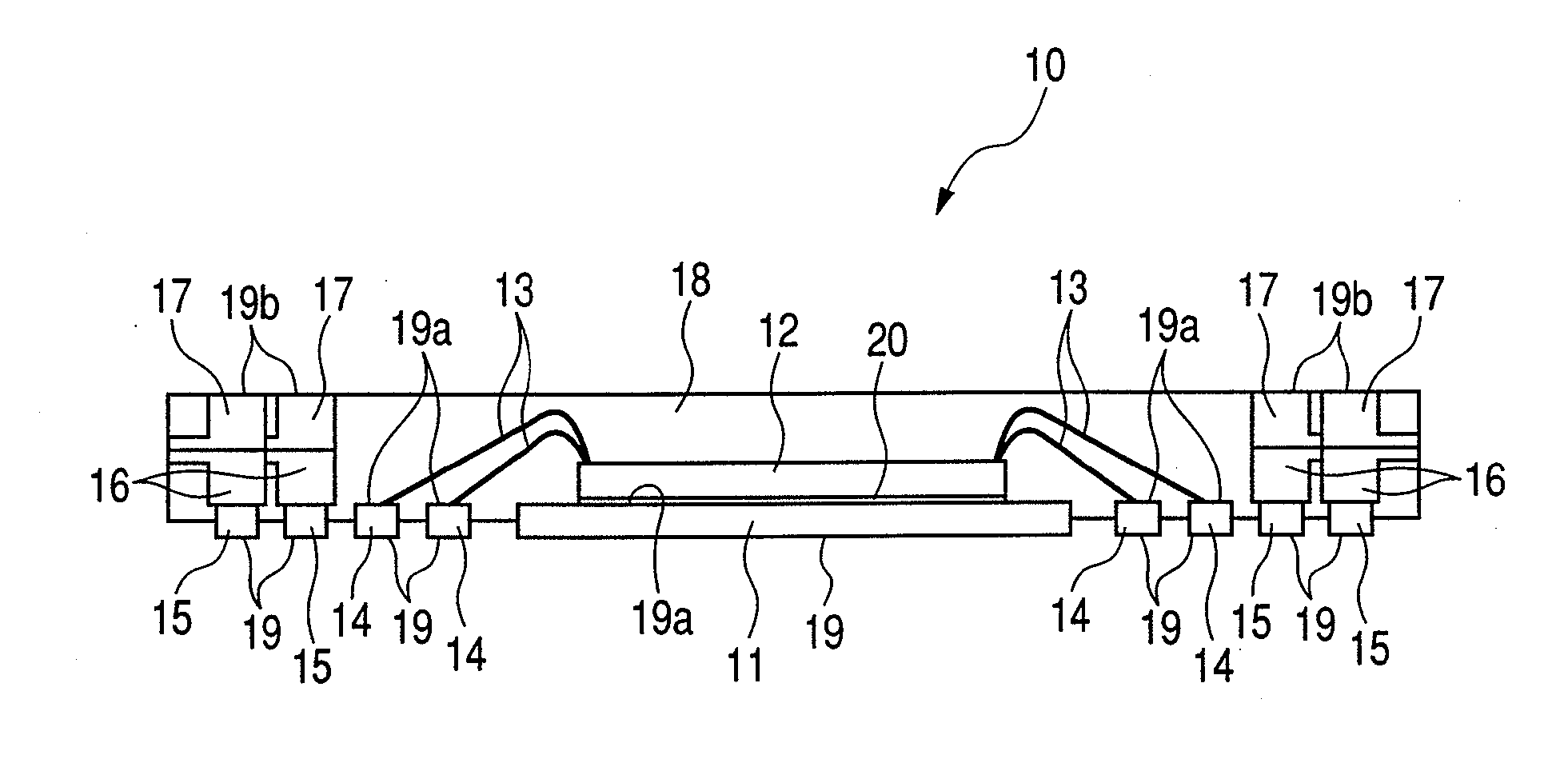
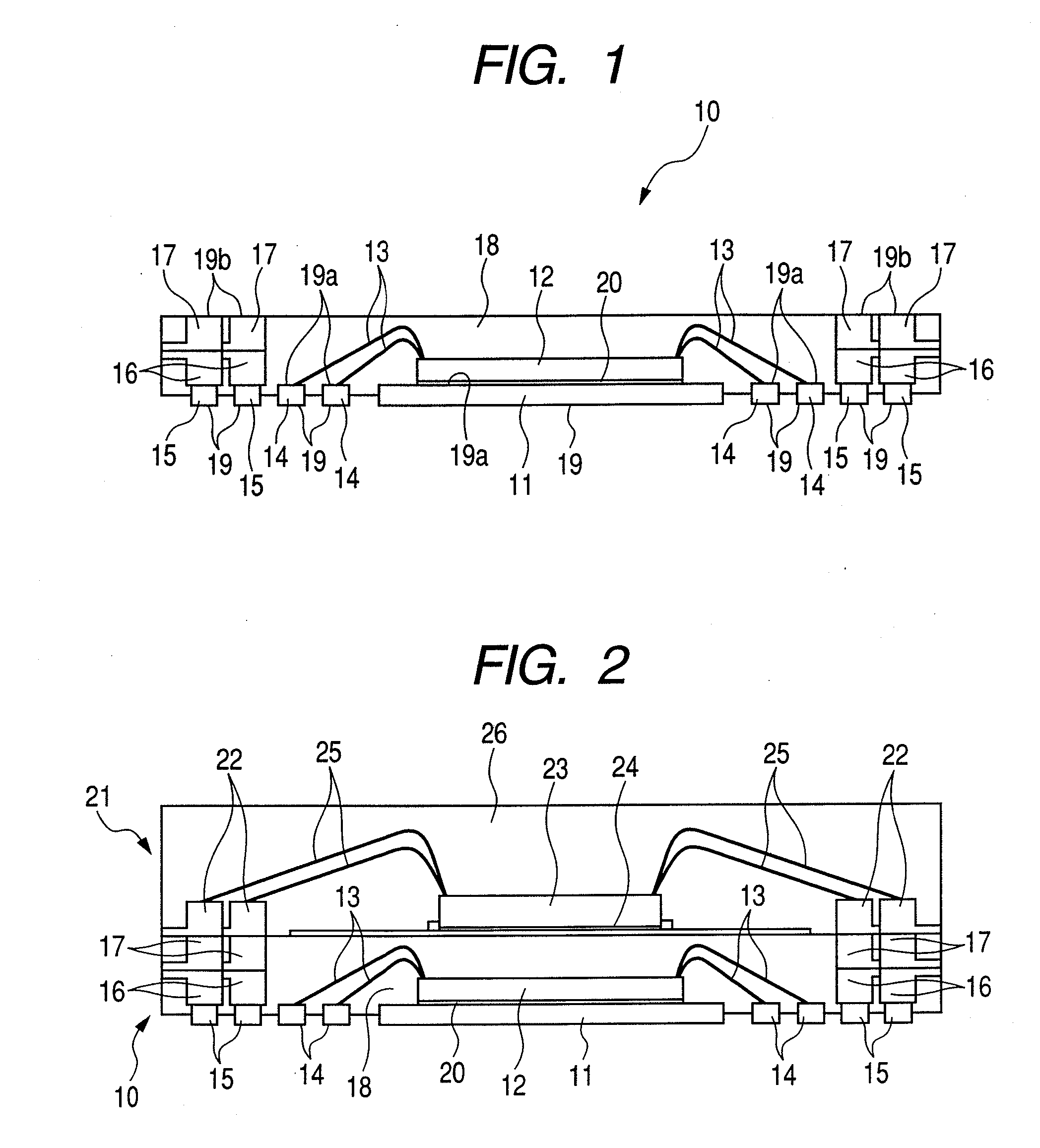
[0104] As shown in FIG. 1, a semiconductor device 10 according to this invention includes a semiconductor element 12 arranged at an internal center and placed on an element mounted portion 11; a group of back-inner terminals 14 connected to some or all of bonding pads of the semiconductor element 12 through bonding wires 13 and exposed to the inside of the bottom so as to be arranged in an area array shape; a group of back-outer terminals 15 arranged outside the group of back-inner terminals 14 and formed in an area array shape; a group of front-outer terminals 17 located immediately above the back-outer terminals 15 and exposed from the front surface, which are electrically connected to the back-outer terminal 15 located immediately below through conductor plates 16 (e.g. copper plates) which are an example of coupling conductors, respectively; and a sealing resin 18 which seals these components (semiconductor element 12, bonding wires 13 and the non-exposed areas of the respective...

second embodiment

[0133] Next, an explanation will be given of the method for manufacturing the semiconductor device 36 according to this invention.

[0134] The method for manufacturing the semiconductor device 36 is different from the method for manufacturing the semiconductor device 10 according to the first embodiment in only the first, third, fifth and eighth steps. So, only the different steps will be explained in details.

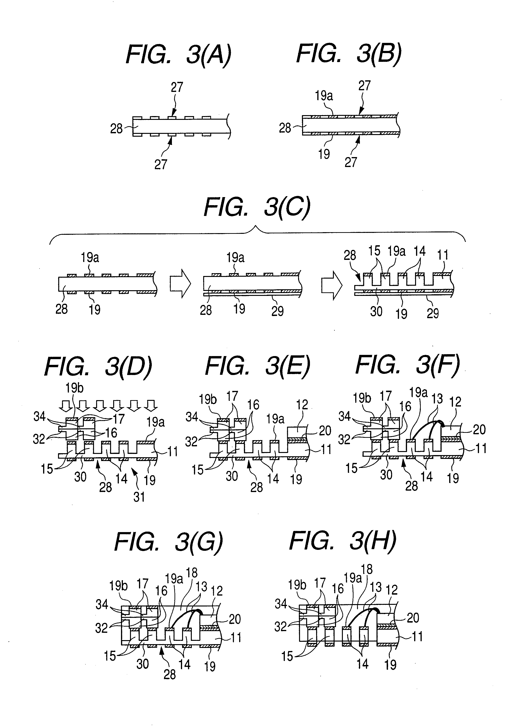
[0135] As shown in FIG. 6A, in the first step, the front and back surfaces of the lead frame material 28 are coated with the resist films 27, respectively and light exposure is done in order to form lead frame patterns each having a group of back-inner terminals 14, a group of back-outer terminals 15, an outer frame (not shown) surrounding these components and leads (not shown) coupling the respective back-inner terminals 14 and back-outer terminals 15 with the outer frame. Further development is done thereby to form the lead frame patterns on the front and back resist films 27....

third embodiment

[0148] Next, an explanation will be given of the method for manufacturing the semiconductor device 39 according to this invention.

[0149] Now, the method for manufacturing the semiconductor device 39 is different from the method for manufacturing the semiconductor device 10 according to the first embodiment in only the fourth, fifth and sixth steps. So, only the different steps will be explained in detail.

[0150] As shown in FIG. 8D, in the fourth step, the semiconductor element 12 is mounted on the element mounted portion 11 through the conductive adhesive layer 20.

[0151] As shown in FIG. 8E, in the fifth step, the respective electrode pads of the semiconductor element 12 are connected to the corresponding back-outer terminals 14 through the bonding wires 13. The respective electrode pads of the semiconductor element 12 are also connected to the bonding wire connecting areas 42 of the corresponding back-outer terminals 15 through the bonding wires 40.

[0152] Further, as shown in FI...


PUM


Abstract

A semiconductor device includes a semiconductor element; a group of back-inner terminals coupled with the semiconductor element through bonding wires and arranged in an area array shape so as to be exposed inside of the bottom; a group of back-outer terminals arranged outside the group of back-inner terminals; a group of front-outer terminals located immediately above the back-outer terminals to be exposed from the front surface, which are electrically coupled with the back-outer terminals located immediately therebelow through coupling conductors, respectively; and a sealing resin which seals the semiconductor element and bonding wires and non-exposed portions of said back-inner terminals, back-outer terminals and front-outer terminals. On at least the respective terminal faces of said back-inner terminals, back-outer terminals and front-outer terminals, noble-metal plated layers are formed.

Description

BACKGROUND OF THE INVENTION [0001] 1. Field of the Invention [0002] This invention relates to a laminated multi-chip module type semiconductor device, a lead-frame product used therefor and a method for manufacturing it. [0003] 2. Related Art [0004] Traditionally, there is a known semiconductor package suited to layered multi-chip module packaging which includes a semiconductor chip, external terminals connected to the electrode pads thereof through lead wires (bonding wires) and a mold part (sealing resin) which seal them with resin, and in which the external terminals consist of at least terminals frames stacked in two layers and are exposed to the three faces of the bottom face, side face and upper face of the mold part (for example, see JP-A-2002-76175). [0005] There is also a known resin-sealed type semiconductor device in which the external terminals provided above and below the semiconductor device are connected to a conductor pattern formed on the mold part by exposing the s...

Claims


Application Information

Patent Timeline
Patent Type & Authority Applications(United States)
IPC IPC(8): H01L23/495H01L21/60
CPCH01L21/4832H01L21/6835H01L23/3107H01L23/49537H01L23/49541H01L23/49582H01L24/28H01L24/48H01L24/49H01L24/83H01L24/85H01L25/105H01L2221/68377H01L2224/131H01L2224/48091H01L2224/48247H01L2224/484H01L2224/49171H01L2224/49433H01L2224/73265H01L2224/83851H01L2224/85001H01L2224/85439H01L2224/85444H01L2924/01004H01L2924/01005H01L2924/01028H01L2924/01029H01L2924/01033H01L2924/01046H01L2924/01047H01L2924/01078H01L2924/01079H01L2924/01082H01L2924/014H01L2924/0781H01L2924/15311H01L2924/18165H01L2924/19043H01L2924/00014H01L2924/01006H01L2224/32245H01L2225/1029H01L2224/2929H01L2224/293H01L2224/78H01L2924/00H01L2924/181H01L2224/45099H01L2224/05599H01L2924/00012H01L23/50H01L23/12
Inventor MATSUNAGA, KIYOSHISHIOYAMA, TAKAOHIRASHIMA, TETSUYUKI
Owner MITSUI HIGH TEC INC
Why Eureka
Try Eureka