Circuit board structure with embedded semiconductor chip and method for fabricating the same

a technology of semiconductor chips and circuit boards, applied in the direction of printed circuit manufacturing, printed circuit aspects, basic electric elements, etc., can solve problems such as compromising product quality, and achieve the effect of reducing warpage and dimension variation

Inactive Publication Date: 2008-03-20
PHOENIX PRECISION TECH CORP
View PDF3 Cites 27 Cited by
  • Summary
  • Abstract
  • Description
  • Claims
  • Application Information

AI Technical Summary

Benefits of technology

[0019]The resin coated element of the present invention is formed by laminating the coarse surface of a metal layer, preferably made by a copper foil, on the dielectric layer, made by a prepreg. Alternatively, an adhesive layer is used to tightly bond the coarse surface of the copper foil and the prepreg together. With a glass fiber-reinforced prepreg functioning as the dielectric layer, problems such as warpage and variation of dimensions are effectively reduced. In the present invention, owing to the combination of the metal layer and dielectric layer, the bonding strength between the composite circuit layer and dielectric layer formed by a thinned metal layer, conductive layer, and electroplated metal layer increases, and thus warpage is unlikely to occur to the circuit board.

Problems solved by technology

However, the difference between the carrier board 11, dielectric layer 13, and circuit layer 14 in terms of the coefficient of thermal expansion (CTE) is so great that warpage is likely to occur due to temperature variation of the process, thus compromising product quality.

Method used


Image

  • Circuit board structure with embedded semiconductor chip and method for fabricating the same
  • Circuit board structure with embedded semiconductor chip and method for fabricating the same
  • Circuit board structure with embedded semiconductor chip and method for fabricating the same

Examples


Embodiment Construction

[0026]The following specific embodiments are provided to illustrate the present invention. Persons skilled in the art can readily gain an insight into other advantages and features of the present invention based on the contents disclosed in this specification.

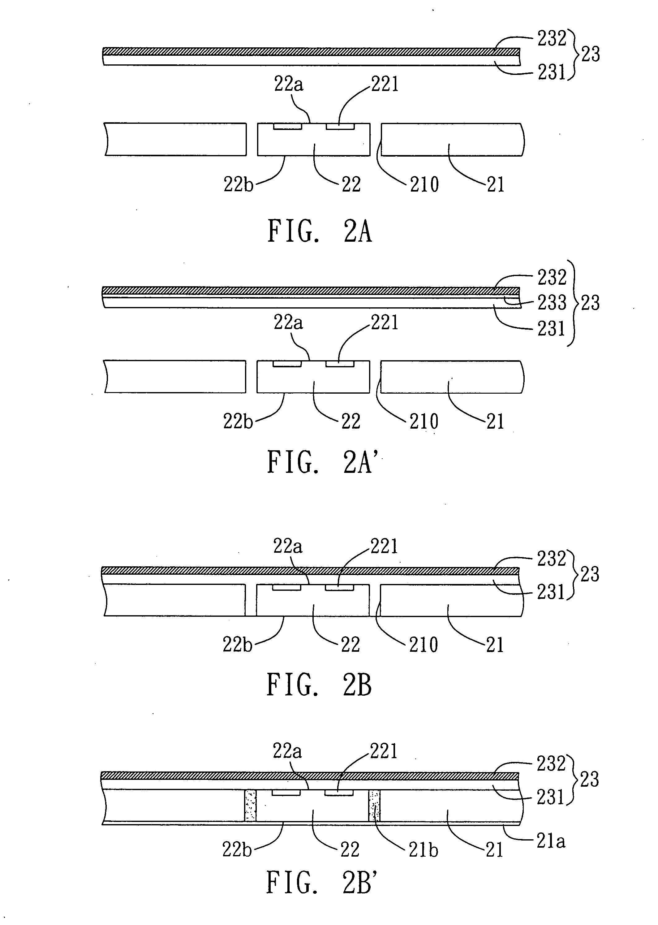
[0027]Referring to FIGS. 2A to 2G, cross-sectional views of a circuit board structure having an embedded semiconductor chip and a method for fabricating the same in accordance with the present invention are provided.

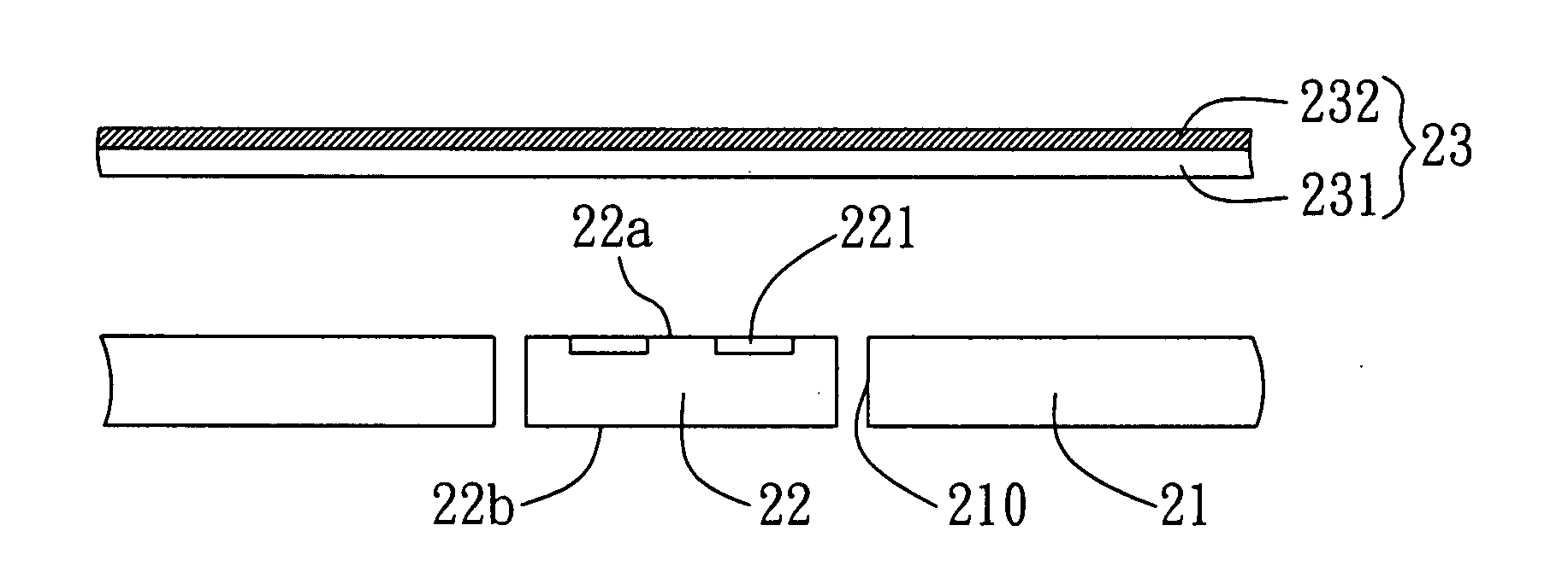
[0028]As shown in FIG. 2A, the method comprises: forming in a carrier board 21 at least one through hole 210 penetrating the carrier board 21, wherein at least one semiconductor chip 22 having an active surface 22a on which a plurality of electrode pads 221 are disposed and a non-active surface 22b opposite to the active surface 22a is received in the through hole 210; providing a resin coated element 23 comprising a dielectric layer 231 and a metal layer 232 formed thereon, wherein the metal layer 232 has a coarse ...


PUM


Abstract

A circuit board structure having an embedded semiconductor chip and a method for fabricating the same are disclosed. The circuit board structure includes: a carrier board formed with at least one through hole; a semiconductor chip received in the through hole of the carrier board, the semiconductor chip having an active surface and a non-active surface, wherein the active surface is provided with a plurality of electrode pads; a dielectric layer formed on surfaces of the carrier board and the semiconductor chip and formed with a plurality of openings for exposing the electrode pads of the semiconductor chip; and a composite circuit layer formed on the dielectric layer, including a thinned metal layer, conductive layer, and electroplated metal layer, and electrically connected to the electrode pads by conductive structures formed in the openings of the dielectric layer. Strong bonding provided by the composite circuit layer formed on the dielectric layer thus desirably reduces the warpage problem resulted from thermal effect.

Description

BACKGROUND OF THE INVENTION[0001]1. Field of the Invention[0002]The present invention relates to circuit board structures, and more particularly, to a circuit board structure with an embedded semiconductor chip and a method for fabricating the same.[0003]2. Description of the Prior Art[0004]Flip chip package technology was introduced into the industry by IBM in the early 1960s. Unlike wire bonding technology, flip chip package technology involves establishing an electrical connection between a semiconductor chip and a substrate via solder bumps instead of gold wires. Flip chip package technology is advantageous because it is capable of increasing package density, reducing the size of the package without the need of using long gold wires, and thus enables better electrical performance of the packaged components.[0005]In recent years, owing to an increasing demand towards high-densitiy, hight-speed and low-cost semiconductor chips, as well as the demand of miniaturization and high int...

Claims


Application Information

Patent Timeline
Patent Type & Authority Applications(United States)
IPC IPC(8): H01L23/48H01L21/4763
CPCH01L21/6835H01L2924/18162H01L2224/92144H01L2924/01079H01L2924/15174H05K1/185H05K1/188H05K3/108H05K3/4652H05K2201/0355H05K2201/09563H05K2201/10674H05K2203/0353H01L24/19H01L2224/04105H01L23/5389H01L2924/3511
Inventor HSU, SHIH-PING
Owner PHOENIX PRECISION TECH CORP
Why Eureka
Try Eureka