

Acoustic wave device, resonator and filter
a technology of acoustic waves and filters, applied in the direction of piezoelectric/electrostrictive devices, device materials, piezoelectric/electrostrictive/magnetostrictive devices, etc., can solve the problems of large loss of acoustic wave devices, and the sharpness of mechanical resonance of the first dielectric film b>14/b> is considerably smaller, so as to improve the temperature coefficient of frequency and improve the effect of loss
- Summary
- Abstract
- Description
- Claims
- Application Information
AI Technical Summary
Benefits of technology
Problems solved by technology
Method used
Image

Examples
first embodiment
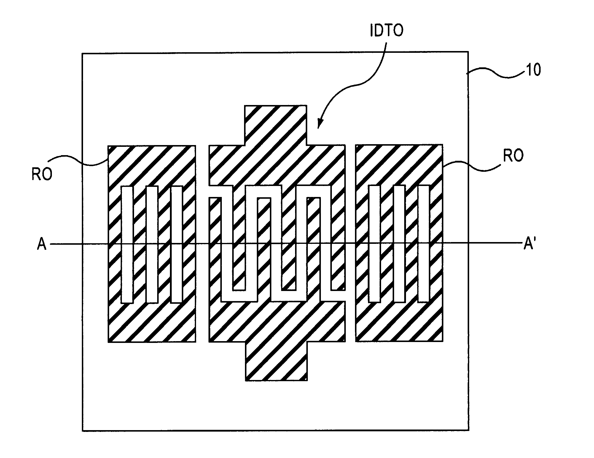
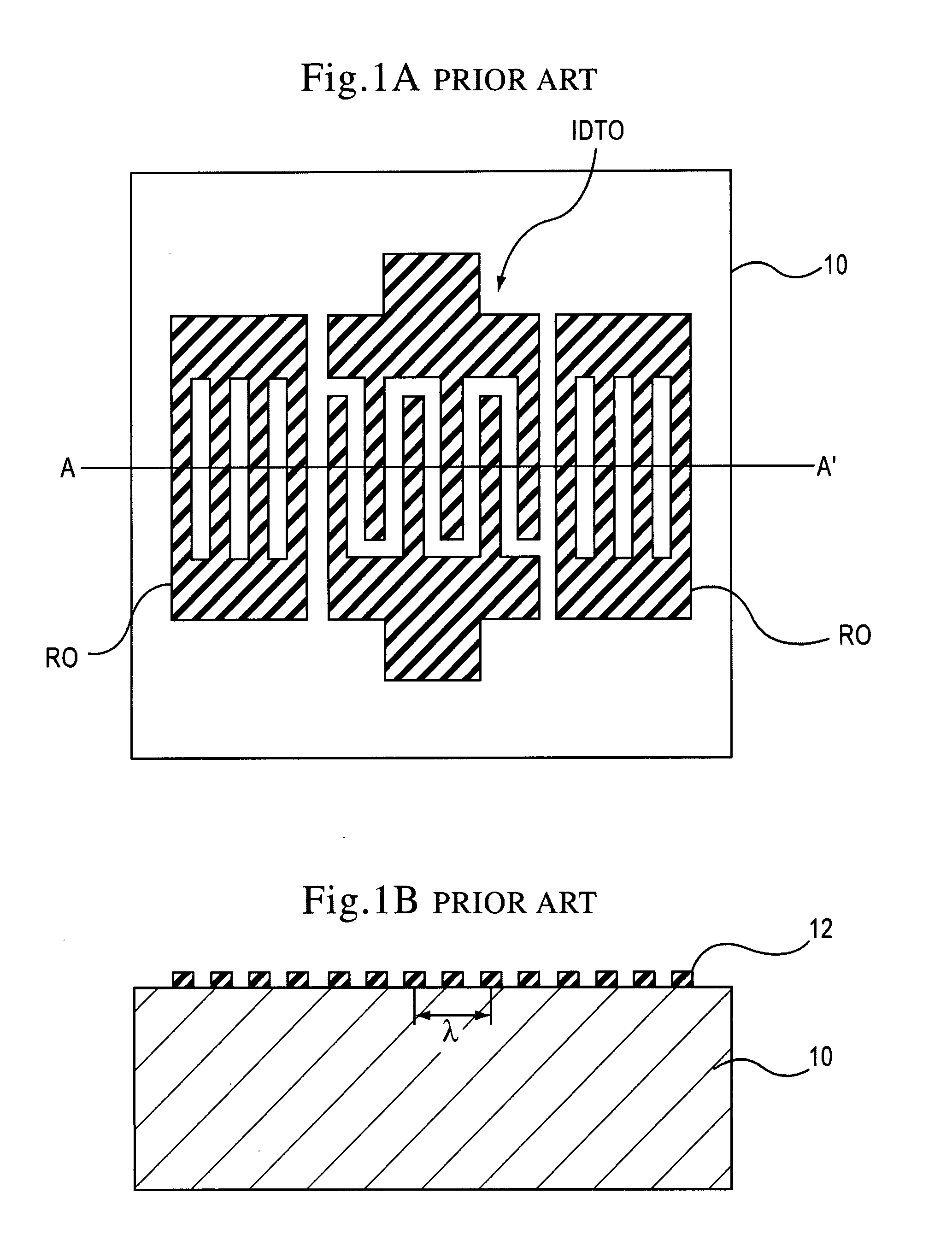
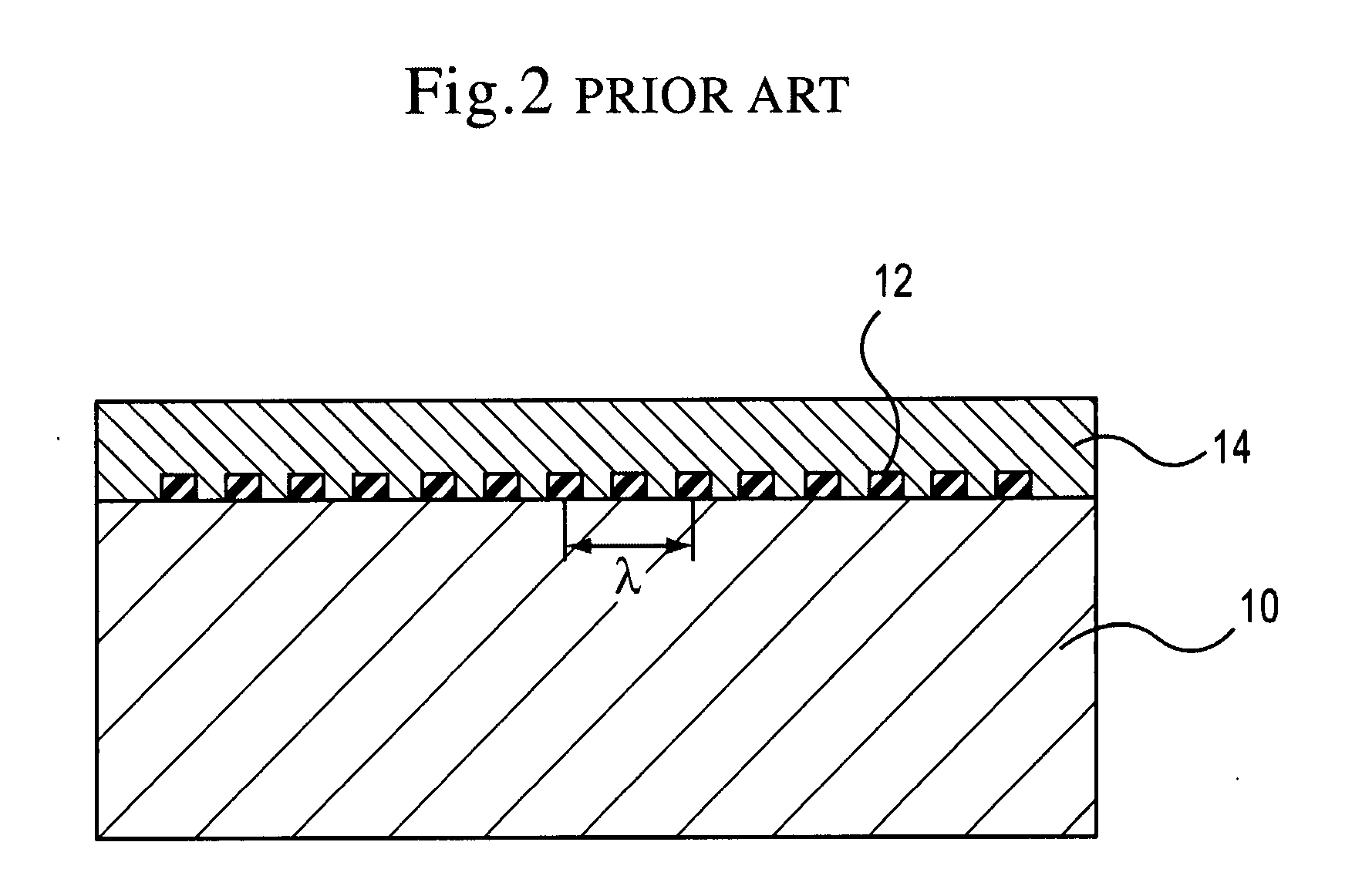
[0042]FIG. 4A is a plan view pf an acoustic wave device according to a first embodiment of the present invention, and FIG. 4B is a cross-sectional view taken along a line A-A′ shown in FIG. 4A. The electrode 12 is provided above, more specifically, provided on the piezoelectric substrate 10, which may, for example, be made of LiNbO3 or LiTaO3. The electrode 12 may, for example, be made of copper. The electrode 12 includes the pair of comb electrodes IDT0 and the pair of reflection electrodes R0 provided at both sides of the pair IDT0 in the propagation direction of the acoustic wave. The comb electrodes IDT0 have a plurality of electrode fingers, and have a cross-section shown in FIG. 4B. The first dielectric film 14 made of silicon oxide is provided so as to cover the electrode 12. The third dielectric film 16 made of aluminum oxide is provided on the third dielectric film 14. The first dielectric film 14 has empty spaces 20a associated with the electrode 12. The empty spaces 20a i...
second embodiment
[0046] A second embodiment has an exemplary structure in which empty spaces are provided not only on the upper surfaces of the electrode but also along side surfaces thereof. FIG. 8 is a cross-sectional view of a resonator in accordance with a second embodiment. Empty spaces 20b are provided on the upper surfaces of the electrode 12 and are provided along the side surfaces thereof. The other structures of the second embodiment are the same as those of the first embodiment shown in FIG. 4B. FIG. 9 shows a structure used in simulation for the second embodiment. The empty spaces 20b has a height of 40 nm from the upper surface of the electrode 12 and a width ha of 30 nm measured from the side surfaces thereof.
[0047]FIG. 10 shows results of computation of the insertion loss [dB] of the second embodiment at the resonance point as a function of the height ha [nm]. It is possible to greatly improve the insertion loss of the resonator by providing the empty spaces 20b so as to contact not ...
third embodiment
[0048] A third embodiment has an exemplary structure in which empty spaces are provided between fingers of the electrode 12. FIG. 11 is a cross-sectional view of a resonator in accordance with a third embodiment. As is shown in FIG. 11, empty spaces 20c are continuously provided between electrode fingers so that opposing side surfaces of adjacent interleaving electrode fingers face each other. In other words, the empty spaces 20c are provided so as to connect the adjacent electrode fingers. The empty spaces 20c are continuous to the electrode fingers. The other structures of the third embodiment are the same as those of the first embodiment shown in FIG. 4B. FIG. 12 shows a structure used in simulation for the third embodiment. The empty spaces 20c have a height 0.2 μm which is equal to the height of the electrode 12.
[0049]FIG. 13 results of computation of the insertion loss [dB] of the third embodiment at the resonance point as a function of the height ha [nm]. The empty spaces 20...
PUM
 Abstract
Description
Claims
Application Information