Semiconductor device and impedance adjusting method thereof

a semiconductor and impedance adjusting technology, applied in the field of impedance adjusting methods, can solve the problems of increasing the area occupied by the circuit for adjusting, and the operation of lower-speed impedance adjusting, and achieve the effect of reducing the area of the impedance adjusting circuit and the operation of higher-speed impedance adjusting

Inactive Publication Date: 2008-03-20
RENESAS ELECTRONICS CORP
View PDF3 Cites 19 Cited by
  • Summary
  • Abstract
  • Description
  • Claims
  • Application Information

AI Technical Summary

Benefits of technology

[0020]The semiconductor device according to the aspect of the present invention comprises the output buffer circuit having the plurality of transistors and the impedance adjusting circuit for adjusting the impedance value of the output buffer circuit. The impedance adjusting circuit includes the impedance measuring circuit for measuring the impedance values of the reference transistor portions including the reference transistors each provided in association with one of the transistor groups including those of the plurality of transistors composing the output buffer circuit which are equal in transistor size and having the same transistor size as the transistors included in the transistor group. In short, the impedance adjusting circuit is constructed to measure the impedance values of the reference transistors and adjust the impedance value of the output buffer circuit based on the result of measurement. This allows a reduction in the area of the impedance adjusting circuit.
[0021]The impedance adjusting method according to the present invention measures the impedance values of the reference transistors within the semiconductor device and generates the output buffer codes for adjusting the impedance value of the output buffer circuit based on the result of the measurement. As a result, it is possible to implement higher-speed impedance adjustment than implemented by a conventional method using an external resistor.

Problems solved by technology

This leads to the problem of an increase in the area occupied by the circuit for adjusting the impedance of the output buffer circuit.
In the structure according to Patent Document 2, a node vzqref for determining a potential for impedance adjustment is coupled to the external resistor, so that a load is increased to result in the problem of a lower-speed impedance adjusting operation.

Method used


Image

  • Semiconductor device and impedance adjusting method thereof
  • Semiconductor device and impedance adjusting method thereof
  • Semiconductor device and impedance adjusting method thereof

Examples


embodiment 1

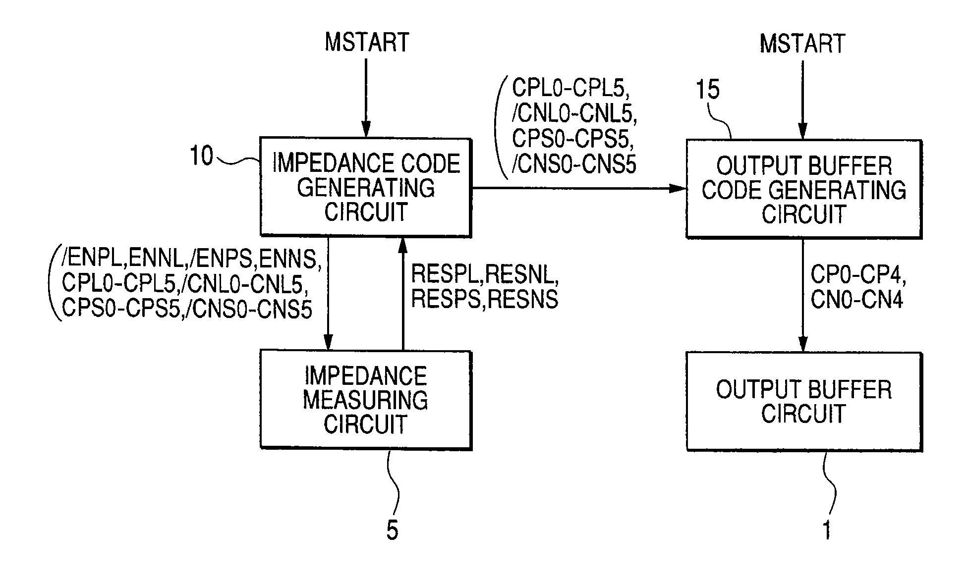
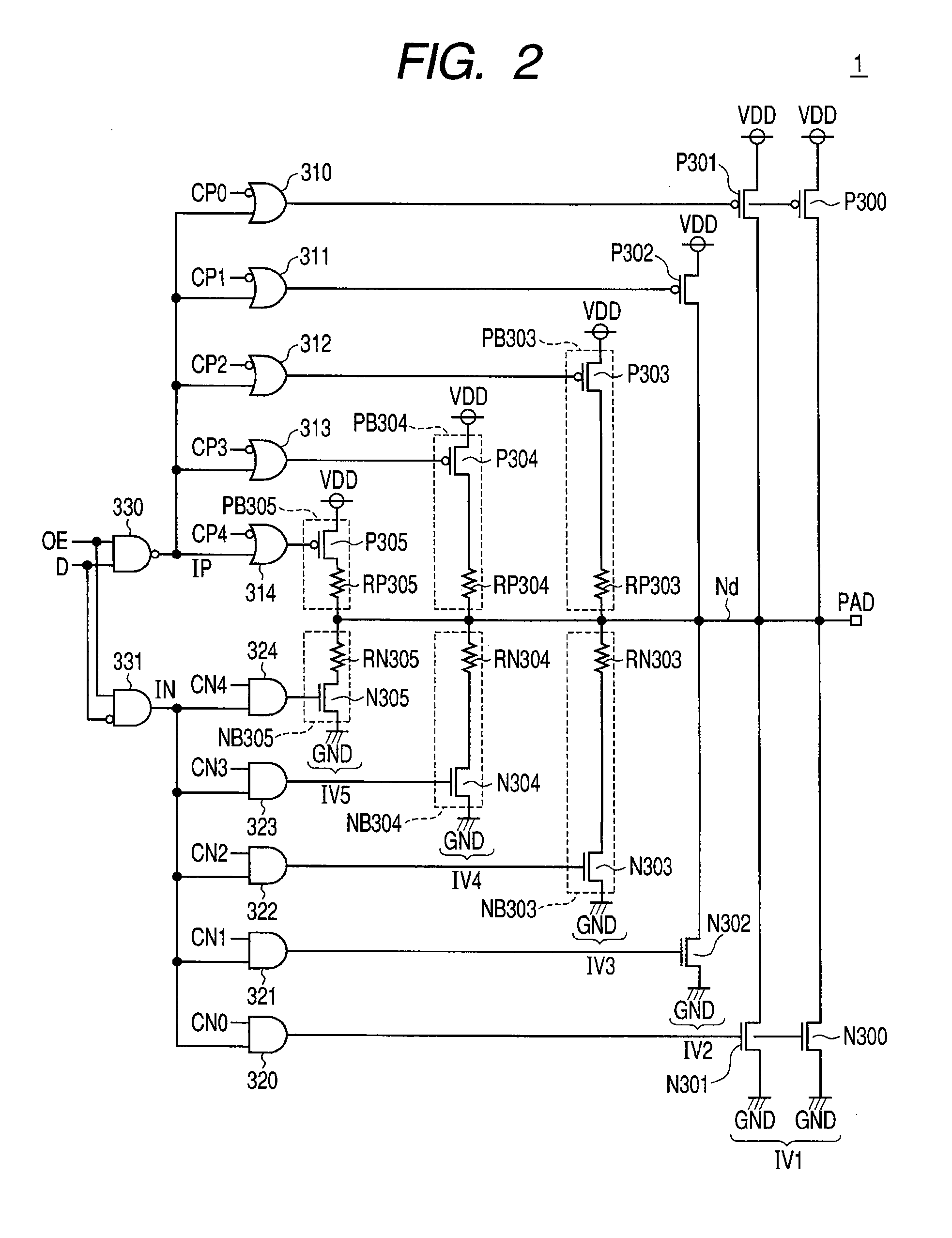
[0039]FIG. 1 is a schematic block diagram of a semiconductor device comprising an output buffer circuit 1 capable of impedance adjustment according to the first embodiment of the present invention.

[0040]Referring to FIG. 1, the semiconductor device according to the first embodiment comprises the output buffer circuit 1, an impedance measuring circuit 5 as an impedance adjusting circuit for adjusting an impedance, an impedance code generating circuit 10 for generating impedance codes based on the result of measurement from the impedance measuring circuit 5, and an output buffer code generating circuit 15 for generating output buffer codes for setting the impedance of the output buffer circuit 1 to a desired value based on the impedance codes from the impedance code generating circuit 10.

[0041]The impedance code generating circuit 10 outputs control signals / ENPL, ENNL, / ENPS, and ENNS to the impedance measuring circuit 5 in response to a control signal MSTART inputted thereto and gen...

embodiment 2

[0210]FIG. 10 is a schematic block diagram of a semiconductor device 1000 according to the second embodiment of the present invention.

[0211]A description will be given to the case where the semiconductor device 1000 according to the second embodiment is coupled to a memory DRAM (Dynamic Random Access Memory) 1001 and various control signals are outputted from a control circuit 20 included in the semiconductor device 1000 to the DRAM 1001.

[0212]Referring to FIG. 10, the semiconductor device 1000 according to the second embodiment comprises the control circuit 20 for outputting the various control signals to the DRAM 1001, output buffer circuits 1 and 1# for outputting the output signals from the control circuit 20 to the DRAM 1001, and impedance adjusting circuits provided in association with the output buffer circuits 1 and 1# to adjust the respective impedances of the output buffer circuits 1 and 1#. The impedance adjusting circuits for the output buffer circuits 1 and 1# include i...

embodiment 3

[0219]The second embodiment shown above has described the method in which the control signal MSTART is also outputted when the control unit 20 outputs the control signal AUTOREF as the auto-refresh command to the DRAM 1001 to simultaneously implement the generation of the impedance codes and the generation of the output buffer codes.

[0220]However, to implement impedance adjustment in the output buffer circuits 1 and 1#, it is necessary to perform impedance measurement, the generation of the impedance codes based on the impedance measurement, and the generation of the output buffer codes based on the impedance codes, as described above. Accordingly, a certain length of period is needed to implement impedance adjustment.

[0221]When consideration is given to the time required to perform impedance measurement, the generation of the impedance codes based on the impedance measurement, and the generation of the output buffer codes based on the impedance codes, there is the possibility that ...


PUM


Abstract

There is provided a semiconductor device including an output buffer circuit which reduces an area occupied by a circuit for impedance adjustment and allows high-speed impedance adjustment. In an impedance measuring circuit, the impedance values of reference transistors having the same sizes as those of a plurality of transistors composing the output buffer circuit which are equal in size are measured. An impedance code generating circuit outputs impedance codes corresponding to the impedance values of the reference transistors to an output buffer code generating circuit based on the result of the measurement from the impedance measuring circuit. The output buffer code generating circuit generates output buffer codes for adjusting the impedance of the output buffer circuit by performing an arithmetic operation process to provide an objective impedance based on the impedance codes.

Description

CROSS-REFERENCE TO RELATED APPLICATIONS[0001]The disclosure of Japanese Patent Application No. 2006-249464 filed on Sep. 14, 2006 including the specification, drawings and abstract is incorporated herein by reference in its entirety.BACKGROUND OF THE INVENTION[0002]The present invention relates to an impedance adjusting method for adjusting an impedance and to a semiconductor device comprising an output buffer circuit capable of adjusting an impedance.[0003]In recent years, as the operating speeds of semiconductor devices have become higher, the speeds of signals propagating along signal lines for performing the transmission and reception of the signals between the plurality of semiconductor devices have also become higher. To implement high-speed data transfer, it is necessary to perform impedance matching in a transmission system and suppress the distortion of a transfer waveform due to reflection and the like. To achieve the impedance matching, there has been conventionally adopt...

Claims


Application Information

Patent Timeline
Patent Type & Authority Applications(United States)
IPC IPC(8): H03K19/0175
CPCH03K19/018578H03K19/0005G11C29/025G11C29/022
Inventor MORISHIMA, CHIKAYOSHIOSAWA, TOKUYAHARAGUCHI, MASARUYAMASHITA, YOSHIHIRO
Owner RENESAS ELECTRONICS CORP
Why Eureka
Try Eureka